©2005 Fairchild Semiconductor Corporation
1
www.fairchildsemi.com
July 2005
Single-channel: 6N137, HCPL-2601, HCPL-2611 Dual-Channel: HCPL-2630, HCPL-2631 Rev. 1.0.3
Single-channel: 6N137, HCPL-2601, HCPL-2611 Dual-Channel: HCPL-2630, HCPL-2631 High Speed-10 MBit/s Logic Gate Optocouplers
Single-channel: 6N137, HCPL-2601, HCPL-2611
Dual-Channel: HCPL-2630, HCPL-2631
High Speed-10 MBit/s Logic Gate Optocouplers
Features
Very high speed-10 MBit/s
Superior CMR-10 kV/µs
Double working voltage-480V
Fan-out of 8 over -40∞C to +85∞C
Logic gate output
Strobable output
Wired OR-open collector
U.L. recognized (File # E90700)
Applications
Ground loop elimination
LSTTL to TTL, LSTTL or 5-volt CMOS
Line receiver, data transmission
Data multiplexing
Switching power supplies
Pulse transformer replacement
Computer-peripheral interface
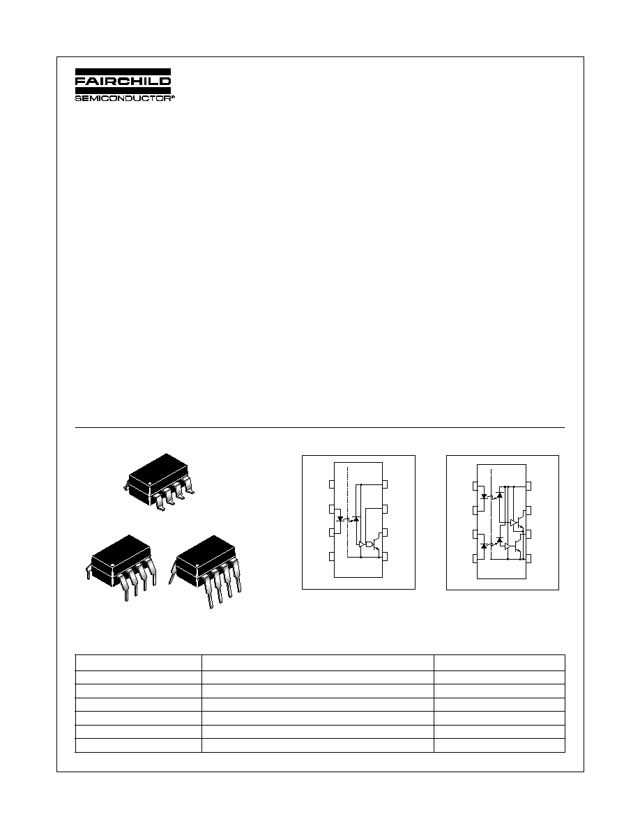
Description
The 6N137, HCPL-2601/2611 single-channel and HCPL-2630/
2631 dual-channel optocouplers consist of a 850 nm AlGaAS
LED, optically coupled to a very high speed integrated photo-
detector logic gate with a strobable output. This output features
an open collector, thereby permitting wired OR outputs. The
coupled parameters are guaranteed over the temperature range
of -40∞C to +85∞C. A maximum input signal of 5 mA will provide
a minimum output sink current of 13mA (fan out of 8).
An internal noise shield provides superior common mode rejec-
tion of typically 10kV/µs. The HCPL- 2601 and HCPL- 2631 has
a minimum CMR of 5 kV/µs. The HCPL-2611 has a minimum
CMR of 10 kV/µs.
Package
Schematic
Truth Table (Positive Logic)
A 0.1µF bypass capacitor must be connected between pins 8 and 5. (See note 1)
8
8
1
8
1
1
1
2
3
4
5
6
7
8
N/C
_
V
CC
V
E
V
O
GND
+
N/C
V
F
1
2
3
4
5
6
7
8
+
_
V
F1
V
CC
V
01
V
02
GND
V
F2
_
+
HCPL-2630
HCPL-2631
6N137
HCPL-2601
HCPL-2611
Input Enable Output
H H L
L H H
H L H
L L H
H NC L
L NC H
2
www.fairchildsemi.com
Single-channel: 6N137, HCPL-2601, HCPL-2611 Dual-Channel: HCPL-2630, HCPL-2631 Rev. 1.0.3
Single-channel: 6N137, HCPL-2601, HCPL-2611 Dual-Channel: HCPL-2630, HCPL-2631 High Speed-10 MBit/s Logic Gate Optocouplers
Absolute Maximum Ratings
(T
A
= 25∞C unless otherwise specified)
Recommended Operating Conditions
*6.3mA is a guard banded value which allows for at least 20% CTR degradation. Initial input current threshold value is
5.0 mA or less.
Parameter
Symbol
Value
Units
Storage Temperature
T
STG
-55 to +125
∞C
Operating Temperature
T
OPR
-40 to +85
∞C
Lead Solder Temperature
T
SOL
260 for 10 sec
∞C
EMITTER
DC/Average Forward
Single Channel
I
F
50
mA
Input Current
Dual Channel (Each Channel)
30
Enable Input Voltage
Not to exceed V
CC
by more than 500 mV
Single Channel
V
E
5.5
V
Reverse Input Voltage
Each Channel
V
R
5.0
V
Power Dissipation
Single Channel
P
I
100
mW
Dual Channel (Each Channel)
45
DETECTOR
Supply Voltage
V
CC
(1 minute max)
7.0
V
Output Current
Single Channel
I
O
50
mA
Dual Channel (Each Channel)
50
Output Voltage
Each Channel
V
O
7.0
V
Collector Output
Single Channel
P
O
85
mW
Power Dissipation
Dual Channel (Each Channel)
60
Parameter
Symbol
Min
Max
Units
Input Current, Low Level
I
FL
0
250
µA
Input Current, High Level
I
FH
*6.3
15
mA
Supply Voltage, Output
V
CC
4.5
5.5
V
Enable Voltage, Low Level
V
EL
0
0.8
V
Enable Voltage, High Level
V
EH
2.0
V
CC
V
Low Level Supply Current
T
A
-40
+85
∞C
Fan Out (TTL load)
N
8
3
www.fairchildsemi.com
Single-channel: 6N137, HCPL-2601, HCPL-2611 Dual-Channel: HCPL-2630, HCPL-2631 Rev. 1.0.3
Single-channel: 6N137, HCPL-2601, HCPL-2611 Dual-Channel: HCPL-2630, HCPL-2631 High Speed-10 MBit/s Logic Gate Optocouplers
Electrical Characteristics
(T
A
= 0 to 70∞C Unless otherwise specified)
Individual Component Characteristics
Switching Characteristics
(T
A
= -40∞C to +85∞C, V
CC
= 5 V, I
F
= 7.5 mA Unless otherwise specified)
Parameter
Test Conditions
Symbol
Min
Typ**
Max
Unit
EMITTER
(I
F
= 10mA)
V
F
1.8
V
Input Forward Voltage
T
A
= 25∞C
1.4
1.75
Input Reverse Breakdown Voltage
(I
R
= 10µA)
B
VR
5.0
V
Input Capacitance
(V
F
= 0, f = 1 MHz)
C
IN
60
pF
Input Diode Temperature Coefficient
(I
F
= 10mA)
V
F
/
T
A
-1.4
mV/∞C
DETECTOR
High Level Supply Current
Single Channel
(V
CC
= 5.5 V, I
F
= 0 mA)
I
CCH
7
10
mA
Dual Channel
(V
E
= 0.5V)
10
15
Low Level Supply Current
Single Channel
(V
CC
= 5.5 V, I
F
= 10 mA)
I
CCL
9
13
mA
Dual Channel
(V
E
= 0.5V)
14
21
Low Level Enable Current
(V
CC
= 5.5 V, V
E
= 0.5V)
I
EL
-0.8
-1.6
mA
High Level Enable Current
(V
CC
= 5.5 V, V
E
= 2.0V)
I
EH
-0.6
-1.6
mA
High Level Enable Voltage
(V
CC
= 5.5 V, I
F
= 10 mA)
V
EH
2.0
V
Low Level Enable Voltage
(V
CC
= 5.5 V, I
F
= 10 mA)(Note 3)
V
EL
0.8
V
AC Characteristics
Test Conditions Symbol
Min
Typ**
Max
Unit
Propagation Delay Time
to Output High Level
(Note 4) (T
A
= 25∞C)
T
PLH
20
45
75
ns
(R
L
= 350
, C
L
= 15 pF) (Fig. 12)
100
Propagation Delay Time
to Output Low Level
(Note 5) (T
A
= 25∞C)
T
PHL
25
45
75
ns
(R
L
= 350
, C
L
= 15 pF) (Fig. 12)
100
Pulse Width Distortion
(R
L
= 350
, C
L
= 15 pF) (Fig. 12)
|T
PHL
-
T
PLH
|
3
35
ns
Output Rise Time
(10-90%)
(R
L
= 350
, C
L
= 15 pF)
(Note 6) (Fig. 12)
t
r
50
ns
Output Rise Time
(90-10%)
(R
L
= 350
, C
L
= 15 pF)
(Note 7) (Fig. 12)
t
f
12
ns
Enable Propagation Delay
Time to Output High Level
(I
F
= 7.5 mA, V
EH
= 3.5 V)
(R
L
= 350
, C
L
= 15 pF) (Note 8) (Fig. 13)
t
ELH
20
ns
Enable Propagation Delay
Time to Output Low Level
(I
F
= 7.5 mA, V
EH
= 3.5 V)
(R
L
= 350
, C
L
= 15 pF) (Note 9) (Fig. 13)
t
EHL
20
ns
Common Mode Transient
Immunity (at Output High
Level)
(T
A
= 25∞C) |V
CM
| = 50V, (Peak)
(I
F
= 0 mA, V
OH
(Min.) = 2.0V)
|CM
H
|
V/µs
6N137, HCPL-2630
HCPL-2601, HCPL-2631
(R
L
= 350
) (Note 10)
(Fig. 14)
5000
10,000
10,000
HCPL-2611
|V
CM
| = 400V
10,000 15,000
Common Mode Transient
Immunity (at Output Low
Level)
(R
L
= 350
) (I
F
= 7.5 mA, V
OL
(Max.) = 0.8V
|CM
L
|
10,000
V/µs
6N137, HCPL-2630
|V
CM
| = 50V (Peak)
HCPL-2601, HCPL-2631 (T
A
= 25∞C)(Note 11)(Fig. 14)
5000
10,000
HCPL-2611(T
A
= 25∞C)
|V
CM
| = 400V
10,000 15,000
4
www.fairchildsemi.com
Single-channel: 6N137, HCPL-2601, HCPL-2611 Dual-Channel: HCPL-2630, HCPL-2631 Rev. 1.0.3
Single-channel: 6N137, HCPL-2601, HCPL-2611 Dual-Channel: HCPL-2630, HCPL-2631 High Speed-10 MBit/s Logic Gate Optocouplers
Transfer Characteristics
(T
A
= -40 to +85∞C Unless otherwise specified)
Isolation Characteristics
(T
A
= -40∞C to +85∞C Unless otherwise specified.)
** All Typicals at V
CC
= 5V, T
A
= 25∞C
NOTES
1.
The V
CC
supply to each optoisolator must be bypassed by a 0.1µF capacitor or larger. This can be either a ceramic or solid
tantalum capacitor with good high frequency characteristic and should be connected as close as possible to the package V
CC
and
GND pins of each device.
2.
Each channel.
3.
Enable Input - No pull up resistor required as the device has an internal pull up resistor.
4.
t
PLH
-Propagation delay is measured from the 3.75 mA level on the HIGH to LOW transition of the input current pulse to the 1.5 V
level on the LOW to HIGH transition of the output voltage pulse.
5.
t
PHL
-Propagation delay is measured from the 3.75 mA level on the LOW to HIGH transition of the input current pulse to the 1.5 V
level on the HIGH to LOW transition of the output voltage pulse.
6. t
r
-Rise time is measured from the 90% to the 10% levels on the LOW to HIGH transition of the output pulse.
7.
t
f
-Fall time is measured from the 10% to the 90% levels on the HIGH to LOW transition of the output pulse.
8.
t
ELH
-Enable input propagation delay is measured from the 1.5 V level on the HIGH to LOW transition of the input voltage pulse to
the 1.5 V level on the LOW to HIGH transition of the output voltage pulse.
9.
t
EHL
-Enable input propagation delay is measured from the 1.5 V level on the LOW to HIGH transition of the input voltage pulse to
the 1.5 V level on the HIGH to LOW transition of the output voltage pulse.
10. CM
H
-The maximum tolerable rate of rise of the common mode voltage to ensure the output will remain in the high state (i.e., V
OUT
> 2.0 V). Measured in volts per microsecond (V/µs).
11. CM
L
-The maximum tolerable rate of rise of the common mode voltage to ensure the output will remain in the low output state (i.e.,
V
OUT
< 0.8 V). Measured in volts per microsecond (V/µs).
12. Device considered a two-terminal device: Pins 1,2,3 and 4 shorted together, and Pins 5,6,7 and 8 shorted together.
DC Characteristics
Test Conditions Symbol
Min
Typ**
Max
Unit
High Level Output Current
(V
CC
= 5.5 V, V
O
= 5.5 V)
(I
F
= 250 µA, V
E
= 2.0 V) (Note 2)
I
OH
100 µA
Low Level Output Current
(V
CC
= 5.5 V, I
F
= 5 mA)
(V
E
= 2.0 V, I
CL
= 13 mA) (Note 2)
V
OL
.35 0.6 V
Input Threshold Current
(V
CC
= 5.5 V, V
O
= 0.6 V,
V
E
= 2.0 V, I
OL
= 13 mA)
I
FT
3 5
mA
Characteristics Test
Conditions Symbol
Min
Typ**
Max
Unit
Input-Output
Insulation Leakage
Current
(Relative humidity = 45%)
(T
A
= 25∞C, t = 5 s)
(V
I-O
= 3000 VDC)
(Note 12)
I
I-O
1.0* µA
Withstand Insulation Test Voltage
(RH < 50%, T
A
= 25∞C)
(Note 12) ( t = 1 min.)
V
ISO
2500 V
RMS
Resistance (Input to Output)
(V
I-O
= 500 V) (Note 12)
R
I-O
10
12
Capacitance (Input to Output)
(f = 1 MHz) (Note 12)
C
I-O
0.6 pF
5
www.fairchildsemi.com
Single-channel: 6N137, HCPL-2601, HCPL-2611 Dual-Channel: HCPL-2630, HCPL-2631 Rev. 1.0.3
Single-channel: 6N137, HCPL-2601, HCPL-2611 Dual-Channel: HCPL-2630, HCPL-2631 High Speed-10 MBit/s Logic Gate Optocouplers
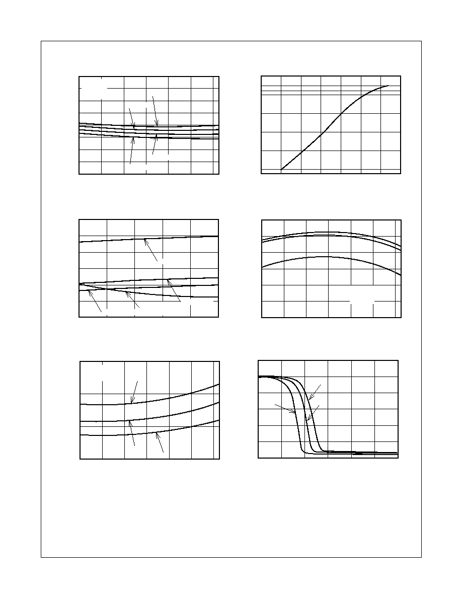
Fig.1 Low Level Output Voltage vs. Ambient Temperature
T
A
- Ambient Temperature (
∞C)
T
A
- Ambient Temperature (
∞C)
T
A
- Ambient Temperature (
∞C)
-40
-20
0
20
40
60
80
V
OL
- Low Level O
utput Voltage
(V)
T
P
- Propagation
Delay (ns)
I
F
- Forward Cur
rent (mA)
I
OL
- Low
Level Output Current (mA)
V
O
- Output Voltage (V)
I
F
- Forward Current (mA)
I
F
- Forward Current (mA)
I
OL
= 16 mA
Fig. 4 Low Level Output Current
vs. Ambient Temperature
-40
-20
0
20
40
60
80
-40
-20
0
20
40
60
80
I
F
= 5 mA
I
F
= 10 mA
I
F
= 15 mA
Fig. 5 Input Threshold Current
vs. Ambient Temperature
I
FT
- Input
Threshold Current (mA)
R
L
= 350
R
L
= 1k
R
L
= 4k
Fig. 6 Output Voltage vs. Input Forward Current
R
L
= 350
R
L
= 1k
R
L
=4k
I
OL
= 6.4 mA
I
OL
= 9.6 mA
I
OL
= 12.8 mA
Conditions:
I
F
= 5 mA
V
E
= 2 V
V
CC
= 5.5V
Conditions:
V
CC
= 5.0 V
V
O
= 0.6 V
Fig. 2 Input Diode Forward Voltage
vs. Forward Current
V
F
- Forward Voltage (V)
0.9
1.0
1.1
1.2
1.3
1.4
1.5
1.6
Conditions:
V
CC
= 5 V
V
E
= 2 V
V
OL
= 0.6 V
Fig.3 Switching Time vs. Forward Current
5
0
1
2
3
4
5
6
7
9
11
13
15
V
CC
= 5 V
R
L
= 1 k
(T
PLH
)
R
L
= 4 k
(T
PLH
)
R
L
= 350
(T
PLH
)
R
L
= 1 k
R
L
= 4 k
R
L
= 350 k
(T
PHL
)
0.0
0.1
0.2
0.3
0.4
0.5
0.6
0.7
0.8
1
2
3
4
0
20
40
60
80
100
120
20
25
30
35
40
45
50
0
1
2
3
4
5
6
0.001
0.01
0.1
1
10
16
30