
PACKAGE
SCHEMATIC
4/29/04
Page 1 of 12
© 2004 Fairchild Semiconductor Corporation
HIGH SPEED
TRANSISTOR OPTOCOUPLERS
HCPL4503M
DESCRIPTION
The HCPL4503M optocoupler consists of an AlGaAs LED optically coupled to a high speed photodetector transistor.
A separate connection for the bias of the photodiode improves the speed by several orders of magnitude over conventional
phototransistor optocouplers by reducing the base-collector capacitance of the input transistor. The base of the phototransistor is
not bonded out to a pin for improved noise immunity.
An internal noise shield provides superior common mode rejection of 15kV/µs minimum.
FEATURES
∑
VISO = 5kV RMS is standard for all devices
∑
High speed-1 MBit/s
∑
Superior CMR, CM
H
= 50 kV/ms (typical); CM
L
= 30 kV/ms (typical)
∑
No base connection for improved noise immunity
∑
CTR guaranteed 0-70∞C
∑
U.L. recognized (File # E90700, Vol 2)
∑
VDE approval pending
APPLICATIONS
∑
Line receivers
∑
Pulse transformer replacement
∑
Output interface to CMOS-LSTTL-TTL
∑
Wide bandwidth analog coupling
8
8
1
8
1
1
1
2
3
4
5
6
7
8
+
_
V
F
V
CC
N/C
V
O
GND
N/C
N/C

4/29/04
Page 2 of 12
© 2004 Fairchild Semiconductor Corporation
HIGH SPEED
TRANSISTOR OPTOCOUPLERS
HCPL4503M
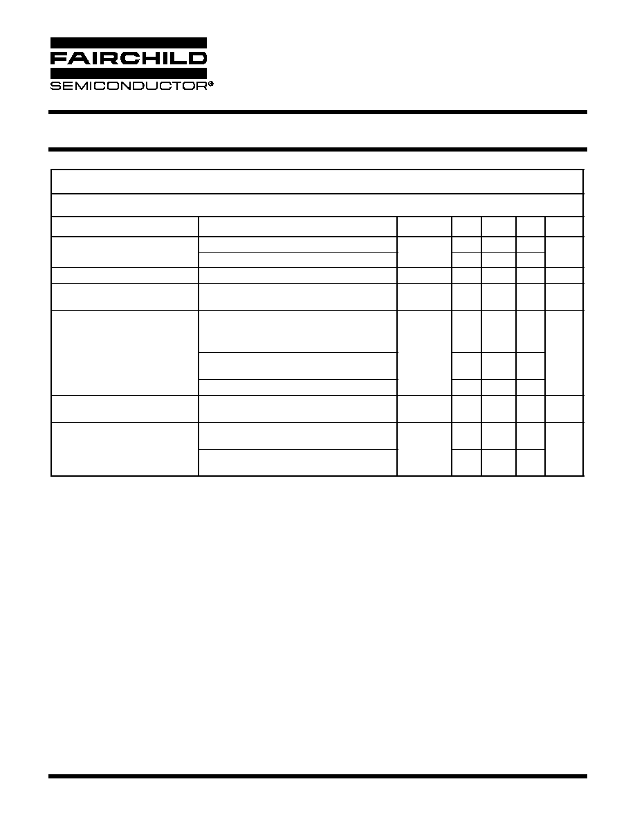
ABSOLUTE MAXIMUM RATINGS
(T
A
= 25∞C unless otherwise specified)
Parameter
Symbol
Value
Units
Storage Temperature
T
STG
-40 to +125
∞C
Operating Temperature
T
OPR
-40 to +100
∞C
Lead Solder Temperature
T
SOL
260 for 10 sec
∞C
EMITTER
DC/Average Forward Input Current
I
F
(avg)
25
mA
Peak Forward Input Current (50% duty cycle, 1 ms P.W.)
I
F
(pk)
50
mA
Peak Transient Input Current - (
1 µs P.W., 300 pps)
I
F
(trans)
1.0
A
Reverse Input Voltage
V
R
5
V
Input Power Dissipation
P
D
100
mW
DETECTOR
Average Output Current
I
O
(avg)
8
mA
Peak Output Current
I
O
(pk)
16
mA
Supply Voltage
V
CC
-0.5 to 30
V
Output Voltage
V
O
-0.5 to 20
V
Output power dissipation
P
D
100
mW
4/29/04
Page 3 of 12
© 2004 Fairchild Semiconductor Corporation
HIGH SPEED
TRANSISTOR OPTOCOUPLERS
HCPL4503M
** All Typicals at T
A
= 25∞C
ELECTRICAL CHARACTERISTICS
(T
A
= 0 to 70∞C Unless otherwise specified)
INDIVIDUAL COMPONENT CHARACTERISTICS
Parameter
Test Conditions
Symbol
Min
Typ**
Max
Unit
EMITTER
(I
F
= 16 mA, T
A
=25∞C)
V
F
1.45
1.7
V
Input Forward Voltage
(I
F
= 16 mA)
1.8
Input Reverse Breakdown Voltage
(I
R
= 10 µA)
B
VR
5.0
V
Temperature coefficient of
forward voltage
(I
F
= 16 mA)
(
V
F
/
T
A
)
-1.6
mV/∞C
DETECTOR
Logic high output current
(I
F
= 0 mA, V
O
= V
CC
= 5.5 V)
(T
A
=25∞C)
I
OH
0.001
0.5
µA
(I
F
= 0 mA, V
O
= V
CC
= 15 V)
(T
A
=25∞C)
0.005
1
(I
F
= 0 mA, V
O
= V
CC
= 15 V)
50
Logic low supply current
(I
F
= 16 mA, V
O
= Open)
(V
CC
= 15 V)
I
CCL
120
200
µA
Logic high supply current
(I
F
= 0 mA, V
O
= Open, V
CC
= 15 V)
(T
A
=25∞C)
I
CCH
1
µA
(I
F
= 0 mA, V
O
= Open)
(V
CC
= 15 V)
2

4/29/04
Page 4 of 12
© 2004 Fairchild Semiconductor Corporation
HIGH SPEED
TRANSISTOR OPTOCOUPLERS
HCPL4503M
** All Typicals at T
A
= 25∞C
** All Typicals at T
A
= 25∞C
TRANSFER CHARACTERISTICS
(T
A
= 0 to 70∞C Unless otherwise specified)
Parameter
Test Conditions
Symbol
Min
Typ**
Max
Unit
COUPLED
(I
F
= 16 mA, V
O
= 0.4 V)
(Note 1) (V
CC
= 4.5 V, T
A
=25∞C)
CTR
19
27
50
%
Current transfer ratio
(Note 5)
(I
F
= 16 mA, V
CC
= 4.5 V, V
OL
=0.5V)
15
30
Logic low output voltage
output voltage
(I
F
= 16 mA, I
O
= 3 mA)
(V
CC
= 4.5 V, T
A
=25∞C)
V
OL
0.5
V
(I
F
= 16 mA, I
O
= 2.4 mA)
(V
CC
= 4.5 V)
0.5
SWITCHING CHARACTERISTICS
(T
A
= 0 to 70∞C unless otherwise specified., V
CC
= 5 V)
Parameter
Test Conditions
Symbol
Min
Typ**
Max
Unit
Propagation delay
time to logic low
(R
L
= 1.9 k
, I
F
= 16 mA) (Note 2) (Fig. 7)
T
A
= 25∞C
T
PHL
0.45
0.8
µs
(R
L
= 1.9 k
, I
F
= 16 mA) (Note 2) (Fig. 7)
1.0
µs
Propagation delay
time to logic high
(R
L
= 1.9 k
, I
F
= 16 mA) (Note 2) (Fig. 7)
T
A
= 25∞C
T
PLH
0.3
0.8
µs
(R
L
= 1.9 k
, I
F
= 16 mA) (Note 2) (Fig. 7)
1.0
µs
Common mode
transient
immunity at
logic high
(I
F
= 0 mA, V
CM
= 1,500 V
P-P
)
T
A
= 25∞C, (R
L
= 1.9 k
)
(Note 3) (Fig. 8)
|CM
H
|
15,000
50,000
V/µs
Common mode
transient
immunity at
logic low
(I
F
= 16 mA, V
CM
= 1,500 V
P-P
)
(R
L
= 1.9 k
)
(Note 3) (Fig. 8)
|CM
L
|
15,000
30,000
V/µs

4/29/04
Page 5 of 12
© 2004 Fairchild Semiconductor Corporation
HIGH SPEED
TRANSISTOR OPTOCOUPLERS
HCPL4503M
Notes
1.
Current Transfer Ratio is defined as a ratio of output collector current, I
O
, to the forward LED input current, I
F
, times 100%.
2.
The 1.9 k
load represents 1 TTL unit load of 1.6 mA and 5.6 k pull-up resistor.
3.
Common mode transient immunity in logic high level is the maximum tolerable (positive) dV
cm
/dt on the leading edge of the
common mode pulse signal V
CM
, to assure that the output will remain in a logic high state (i.e., V
O
>2.0 V). Common mode
transient immunity in logic low level is the maximum tolerable (negative) dV
cm
/dt on the trailing edge of the common mode
pulse signal, V
CM
, to assure that the output will remain in a logic low state (i.e., V
O
<0.8 V).
4.
Device is considered a two terminal device: Pins 1, 2, 3 and 4 are shorted together and Pins 5, 6, 7 and 8 are shorted
together.
ISOLATION CHARACTERISTICS
(T
A
= 0 to 70∞C Unless otherwise specified)
Characteristics
Test Conditions
Symbol
Min
Typ**
Max
Unit
Input-output
insulation leakage current
(Relative humidity = 45%)
(T
A
= 25∞C, t = 5 s)
(V
I-O
= 3000 VDC)
(Note 4)
I
I-O
1.0
µA
Withstand insulation test voltage
(RH
50%, T
A
= 25∞C)
(Note 4) ( t = 1 min.)
V
ISO
5,000
V
RMS
Resistance (input to output)
(Note 9) (V
I-O
= 500 VDC)
R
I-O
10
12
Capacitance (input to output)
(Note 4) (f = 1 MHz)
C
I-O
0.6
pF
4/29/04
Page 6 of 12
© 2004 Fairchild Semiconductor Corporation
HIGH SPEED
TRANSISTOR OPTOCOUPLERS
HCPL4503M
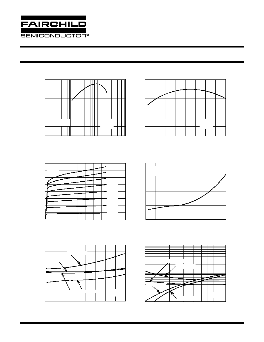
Fig. 1 Normalized CTR vs. Forward Current
I
F
- FORWARD CURRENT (mA)
0.1
1
10
100
NORMALIZED CTR
0.0
0.2
0.4
0.6
0.8
1.0
1.2
Fig. 2 Normalized CTR vs. Temperature
T
A
- TEMPERATURE (
∞C)
-60
-40
-20
0
20
40
60
80
100
NORMALIZED CTR
0.0
0.2
0.4
0.6
0.8
1.0
1.2
Fig. 3 Output Current vs. Output Voltage
V
O
- OUTPUT VOLTAGE (V)
0
2
4
6
8
10
12
14
16
18
20
I
O
- OUTPUT CURRENT (mA)
0
2
4
6
8
10
12
14
16
I
F
= 5 mA
I
F
= 10 mA
I
F
= 15 mA
I
F
= 20 mA
I
F
= 25 mA
I
F
= 30 mA
I
F
= 35 mA
I
F
= 40 mA
Normalized to:
I
F
= 16 mA
V
O
= 0.4 V
V
CC
= 5 V
T
A
= 25
∞C
Normalized to:
T
A
= 25
∞C
I
F
= 16mA
V
CC
= 5 V
V
O
= 0.4 V
Fig. 4 Logic High Output Current
vs. Temperature
T
A
- TEMPERATURE (
∞C)
-60
-40
-20
0
20
40
60
80
100
I
OH
- LOGIC HIGH OUTPUT CURRENT (nA)
0.1
1
10
100
1000
Fig. 5 Propagation Delay vs. Temperature
T
A
- TEMPERATURE (
∞C)
-60
-40
-20
0
20
40
60
80
100
T
p
- PR
OP
A
G
A
TION DELA
Y (ns)
0
100
200
300
400
500
600
700
800
R
L
= 1.9 K (TPHL)
R = 4.1 K (TPLH)
L
R
L
= 1.9 K (TPLH)
R
L
= 4.1 K (TPLH)
Fig. 6 Propagation Delay vs. Load Resistance
R
L
= LOAD RESISTANCE (k
)
1
10
T
P
- PR
OP
A
G
A
TION DELA
Y (ns)
100
1000
10000
IF - 16 mA (TPHL)
IF - 10 mA (TPHL)
IF - 10 mA (TPLH)
IF - 16 mA (TPLH)
T
A
= 25
∞C
V
CC
= 5 V
I
F
= 0 mA
V
CC
= 5 V
V
O
= 5 V
I
F
= 16 mA
V
CC
= 5 V
V
CC
= 5 V
T
A
= 25
∞C

4/29/04
Page 7 of 12
© 2004 Fairchild Semiconductor Corporation
HIGH SPEED
TRANSISTOR OPTOCOUPLERS
HCPL4503M
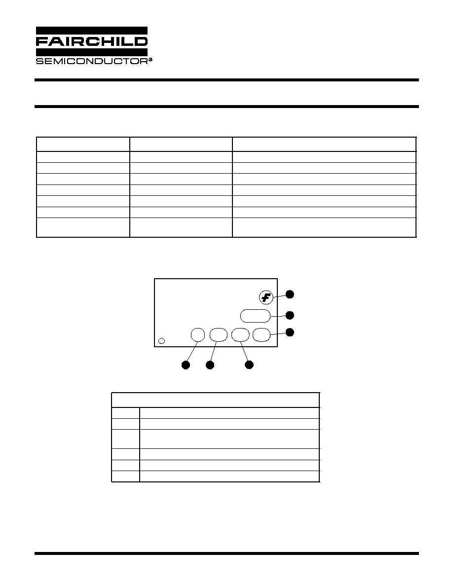
Pulse Gen
CM
V
V
FF
B
A
+
-
+5 V
O
V
-
I
F
3
4
+
F
V
-
2
1
Shield
Noise
6
O
5
GND
7
8
V
N/C
CC
V
L
R
PLH
OL
V
V
O
0
5 V
1.5 V
F
I
1.5 V
T
PHL
T
Switch at A : I = 0 mA
F
Switch at A : I = 16 mA
F
t
r
V
O
O
V
OL
V
5 V
0 V
10%
10%
90%
CM
V 10 V
3
I Monitor
F
4
I/f
< 100µs
10% D.C.
tr = 5ns
Generator
Pulse
Z = 50
O
+
V
F
I
F
-
2
1
Shield
Noise
V
O
O
6
5
GND
7
8
V
N/C
L
R
CC
V
+5 V
0.1
µF
L
C = 1.5
µF
0.1
µF
f
t
m
R
90%
Fig. 8 Common Mode Immunity Test Circuit
Fig. 7 Switching Time Test Circuit

4/29/04
Page 8 of 12
© 2004 Fairchild Semiconductor Corporation
HIGH SPEED
TRANSISTOR OPTOCOUPLERS
HCPL4503M
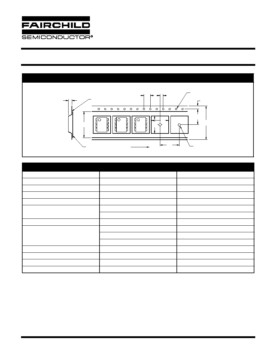
Package Dimensions (Through Hole)
0.200 (5.08)
0.140 (3.55)
0.100 (2.54) TYP
0.022 (0.56)
0.016 (0.41)
0.020 (0.51) MIN
0.390 (9.91)
0.370 (9.40)
0.270 (6.86)
0.250 (6.35)
3
0.070 (1.78)
0.045 (1.14)
2
4
1
5
6
7
8
0.300 (7.62)
TYP
0.154 (3.90)
0.120 (3.05)
0.016 (0.40)
0.008 (0.20)
15∞ MAX
PIN 1
ID.
SEATING PLANE
Package Dimensions (Surface Mount)
Lead Coplanarity : 0.004 (0.10) MAX
0.270 (6.86)
0.250 (6.35)
0.390 (9.91)
0.370 (9.40)
0.022 (0.56)
0.016 (0.41)
0.100 (2.54)
TYP
0.020 (0.51)
MIN
0.070 (1.78)
0.045 (1.14)
0.300 (7.62)
TYP
0.405 (10.30)
MIN
0.315 (8.00)
MIN
0.045 [1.14]
3
2
1
4
5
6
7
8
0.016 (0.41)
0.008 (0.20)
PIN 1
ID.
Package Dimensions (0.4"Lead Spacing)
0.200 (5.08)
0.140 (3.55)
0.100 (2.54) TYP
0.022 (0.56)
0.016 (0.41)
0.004 (0.10) MIN
0.390 (9.91)
0.370 (9.40)
0.270 (6.86)
0.250 (6.35)
3
0.070 (1.78)
0.045 (1.14)
2
4
1
5
6
7
8
0.400 (10.16)
TYP
0.154 (3.90)
0.120 (3.05)
0.016 (0.40)
0.008 (0.20)
0∞ to 15∞
PIN 1
ID.
SEATING PLANE
8 - Pin Dip
0.070 (1.78)
0.060 (1.52)
0.030 (0.76)
0.100 (2.54)
0.295 (7.49)
0.415 (10.54)
NOTE
All dimensions are in inches (millimeters)
4/29/04
Page 9 of 12
© 2004 Fairchild Semiconductor Corporation
HIGH SPEED
TRANSISTOR OPTOCOUPLERS
HCPL4503M
ORDERING INFORMATION
MARKING INFORMATION
Option
Example Part Number
Description
S
HCPL4503SM
Surface Mount Lead Bend
SD
HCPL4503SDM
Surface Mount; Tape and reel (1,000 units per reel)
T
HCPL4503TM
0.4" Lead Spacing
V
HCPL4503VM
VDE0884 (approval pending)
TV
HCPL4503TVM
VDE0884 (approval pending); 0.4" lead spacing
SV
HCPL4503SVM
VDE0884 (approval pending); surface mount
SDV
HCPL4503SDVM
VDE0884 (approval pending); surface mount; tape and reel
(1,000 units per reel)
1
2
6
4
3
5
Definitions
1
Fairchild logo
2
Device number
3
VDE mark (Note: Only appears on parts ordered with VDE
option ≠ See order entry table)
4
Two digit year code, e.g., `03'
5
Two digit work week ranging from `01' to `53'
6
Assembly package code
4503
TB
YY
XX
V
4/29/04
Page 10 of 12
© 2004 Fairchild Semiconductor Corporation
HIGH SPEED
TRANSISTOR OPTOCOUPLERS
HCPL4503M
Carrier Tape Specifications
Description
Symbol
Dimension in mm
Tape Width
W
16.0 ± 0.3
Tape Thickness
t
0.30 ± 0.05
Sprocket Hole Pitch
P
0
4.0 ± 0.1
Sprocket Hole Diameter
D
0
1.55 ± 0.05
Sprocket Hole Location
E
1.75 ± 0.10
Pocket Location
F
7.5 ± 0.1
P
2
4.0 ± 0.1
Pocket Pitch
P
12.0 ± 0.1
Pocket Dimensions
A
0
10.30 ±0.20
B
0
10.30 ±0.20
K
0
4.90 ±0.20
Cover Tape Width
W
1
1.6 ± 0.1
Cover Tape Thickness
d
0.1 max
Max. Component Rotation or Tilt
10∞
Min. Bending Radius
R
30
d
0
P
t
2
D
0
1
1
W
User Direction of Feed
0
K
B
0
A
0
W
E
D
F
P
P

4/29/04
Page 11 of 12
© 2004 Fairchild Semiconductor Corporation
HIGH SPEED
TRANSISTOR OPTOCOUPLERS
HCPL4503M
Reflow Profile
∑ Peak reflow temperature: 260
C (package surface temperature)
∑ Time of temperature higher than 183
C for 160 seconds or less
∑ One time soldering reflow is recommended
245
C, 10≠30 s
Time (Minute)
0
300
250
200
150
100
50
0
0.5
1
1.5
2
2.5
3
3.5
4
4.5
Temperature (∞C)
Time above 183
C, <160 sec
Ramp up = 2≠10
C/sec
260
C peak

LIFE SUPPORT POLICY
FAIRCHILD'S PRODUCTS ARE NOT AUTHORIZED FOR USE AS CRITICAL COMPONENTS IN LIFE SUPPORT DEVICES
OR SYSTEMS WITHOUT THE EXPRESS WRITTEN APPROVAL OF THE PRESIDENT OF FAIRCHILD SEMICONDUCTOR
CORPORATION. As used herein:
1. Life support devices or systems are devices or systems
which, (a) are intended for surgical implant into the body, or
(b) support or sustain life, and (c) whose failure to perform
when properly used in accordance with instructions for use
provided in the labeling, can be reasonably expected to
result in a significant injury of the user.
2. A critical component in any component of a life support
device or system whose failure to perform can be
reasonably expected to cause the failure of the life support
device or system, or to affect its safety or effectiveness.
DISCLAIMER
FAIRCHILD SEMICONDUCTOR RESERVES THE RIGHT TO MAKE CHANGES WITHOUT FURTHER NOTICE TO
ANY PRODUCTS HEREIN TO IMPROVE RELIABILITY, FUNCTION OR DESIGN. FAIRCHILD DOES NOT ASSUME
ANY LIABILITY ARISING OUT OF THE APPLICATION OR USE OF ANY PRODUCT OR CIRCUIT DESCRIBED HEREIN;
NEITHER DOES IT CONVEY ANY LICENSE UNDER ITS PATENT RIGHTS, NOR THE RIGHTS OF OTHERS.
4/29/04
Page 12 of 12
© 2004 Fairchild Semiconductor Corporation
HIGH SPEED
TRANSISTOR OPTOCOUPLERS
HCPL4503M