Rev. 2.5 1/2/03
www.fairchildsemi.com
V
IN
Top View
V
SS
V
OUT
2
1
3
V
IN
V
SS
V
OUT
2
1
3
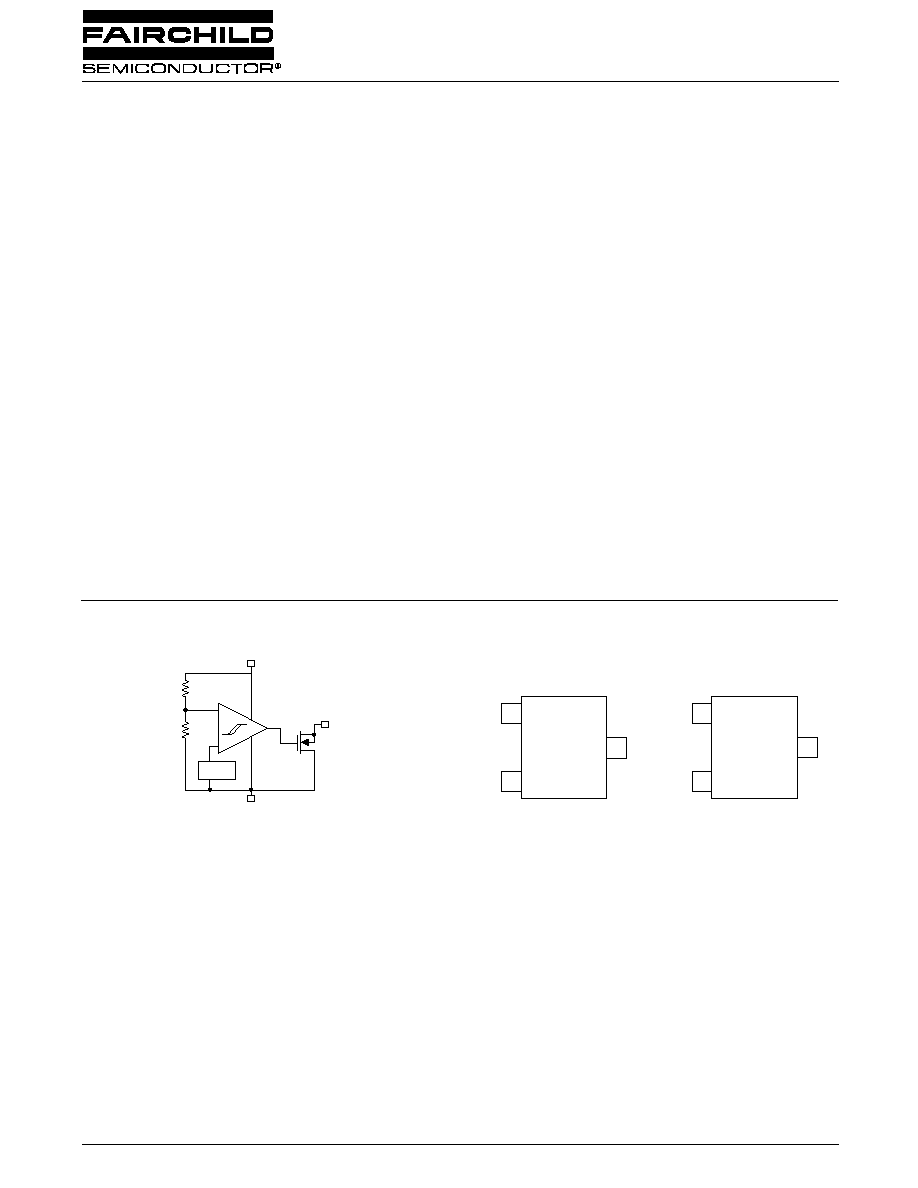
SC-70
SOT-23
Features
∑ All-CMOS design in SOT-23 or SC70 package
∑ ±1% precision in Reset Detection
∑ Only 1µA of Iq
∑ 2mA of sink current capability
∑ Built-in hysteresis of 5% of detection voltage
∑ Voltage options of 2.6, 2.9, 3.1, 4.4, and 4.6V fit most
supervisory applications
∑ Open-Drain Reset Output
Applications
∑ Microprocessor reset circuits
∑ Memory battery back-up circuitry
∑ Power-on reset circuits
∑ Portable and battery powered electronics
Description
All-CMOS Monitor circuits in either a 3-lead SOT-23 or
SC70 package offer the best performance in power con-
sumption and accuracy.
The ILC5061 comes in a series of ±1% accurate trip voltages
to fit most microprocessor applications. Even though its out-
put can sink 2mA, the device draws only 1µA in normal
operation.
Additionally, a built-in hysteresis of 5% of detect voltage
simplifies system design.
ILC5061
Power Supply reset Monitor with 1% Precision
Block Diagram
Pin Package Configurations
V
REF
V
OUT
V
SS
V
IN
2
Rev. 2.5 1/2/03
ILC5061
PRODUCT SPECIFICATION
Electrical Characteristics
T
A
= 25∞C
Parameter
Symbol
Conditions
Min
Type
Max
Units
Detect Fail Voltage
V
DF
V
DF
X 0.99
V
DF
V
DF
X 1.01
V
Hysteresis Range
V
HYS
V
DF
X 0.02
V
DF
X 0.05
V
DF
X 0.08
V
Supply Current
I
SS
V
IN
= 1.5V
V
IN
= 2.0V
V
IN
= 3.0V
V
IN
= 4.0V
V
IN
= 5.0V
0.9
1.0
1.3
1.6
2.0
2.6
3.0
3.4
3.8
4.2
µA
Operating Voltage
V
IN
V
DF
= 2.1~ 6.0V
1.5
10.0
V
Output Current
I
OUT
N-ch
V
DS
= 0.5V
V
IN
= 1.0V
V
IN
= 2.0V
V
IN
= 3.0V
V
IN
= 4.0V
V
IN
= 5.0V
2.2
7.7
10.1
11.5
13.0
mA
Temperature Charac-
teristics
D
V
DF
/(
D
T
opr
*
V
DF
) -30
o
C<T
opr
<80
o
C
-200
+100
+200
Ppm/
o
C
Delay Time Release
Voltage Output Inver-
sion)
T
DLY
(V
DR
to V
OUT
inversion)
0.1
ms
Note:
1. An additional resistor between the V
IN
pin and supply voltage may cause deterioration of the characteristics due
to increasing V
DR.
Absolute Maximum Ratings
Parameter
Symbol
Ratings
Units
Input Voltages
V
IN
12
V
Output Current
I
OUT
50
mA
Output Voltages
V
OUT
V
SS
-0.3~+V
IN
+03
V
Continuous Total
Power Dissipation
SOT 23
P
d
150
mW
Operation Ambient temperature
T
opr
-30~+80
o
C
Storage Temperature
T
stg
-40~+125
o
C
ILC5061
Rev. 2.5 1/2/03
3
PRODUCT SPECIFICATION
ILC5061
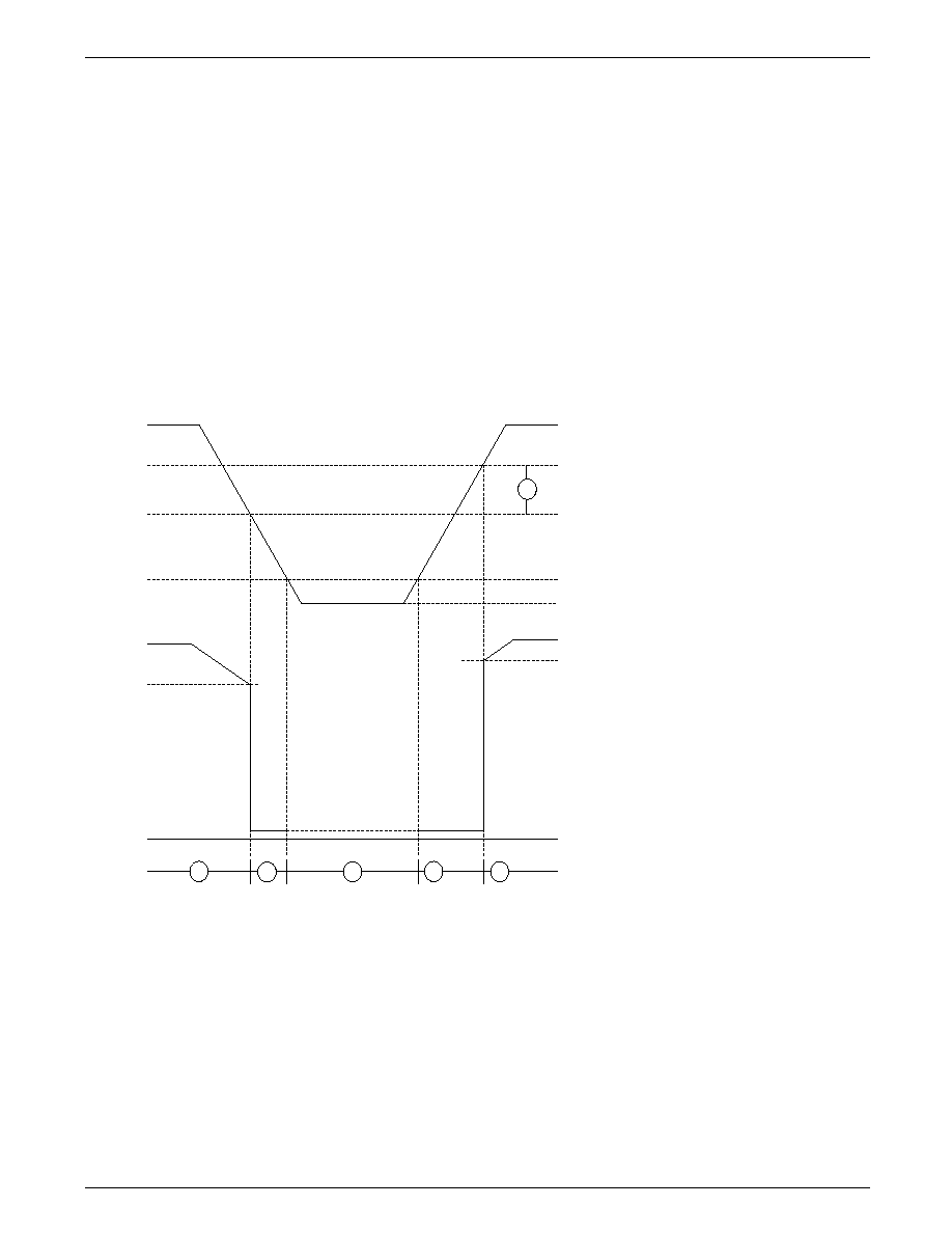
Functional Description
6
5
4
3
1
2
INPUT VOLTAGE (V
IN
)
DETECT RELEASE VOLTAGE (V
DR
)
DETECT FAIL VOLTAGE (V
DF
)
MINIMUM OPERATING VOLTAGE (V
MIN
)
GROUND VOLTAGE (V
SS
)
OUTPUT VOLTAGE (V
OUT
)
GROUND VOLTAGE (V
SS
)
The following designators 1~6 refer to the timing diagram below.
1. While the input voltage (V
IN
) is higher than the detect voltage (V
DF
), the V
OUT
output pin is at high impedance
state.
2. When the input V
IN
voltage falls lower than V
DF
, V
OUT
drops near to ground voltage
3. If the input voltage further decreases below the minimum operating voltage (V
MIN
), the V
OUT
output becomes
unstable. In this condition, if the V
OUT
pin is pulled up, V
OUT
indicates the V
IN
voltage.
4. During an increase of the input voltage from the V
SS
voltage, V
OUT
is not stable in the voltage below the V
MIN
.
Exceeding that level, the output stays at the ground level (V
SS
) between the minimum operating voltage (V
MIN
)
and the detect release voltage (V
DR
).
5. If the input voltage increases more than V
DR
, then the V
OUT
output pin is at high impedance state.
6. The difference between V
DR
and V
DF
is the hysteresis in the system.
4
Rev. 2.5 1/2/03
ILC5061
PRODUCT SPECIFICATION
Ordering Information
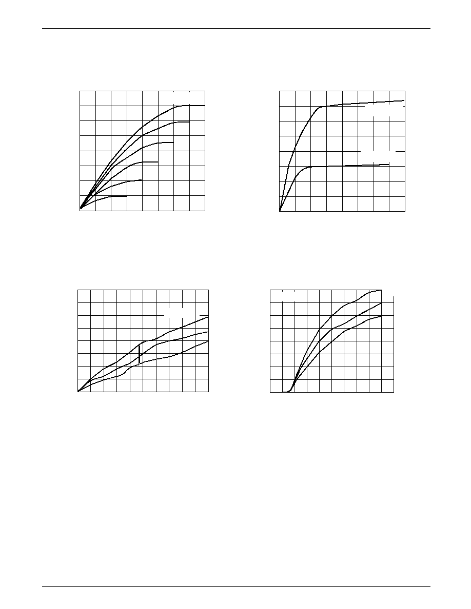
Typical Performance Characteristics
(General conditions for all curves)
70
0
1
2
3
4
ILC5061
Output Voltage vs Output Current
OUTPUT CURRENT I
OUT
(mA)
OUTPUT VOLTAGE V
OUT
(V)
50
10
0
20
30
40
60
80
V
IN
= 4.0V
3.5V
3.0V
2.5V
2.0V
1.5V
0
0.2
0.4
0.6
0.8
ILC5061
Output Voltage vs Output Current
OUTPUT CURRENT I
OUT
(
µ
A)
OUTPUT VOLTAGE V
OUT
(V)
0
200
400
600
800
V
IN
= 0.8V
V
IN
= 0.7V
0
2
4
6
8
ILC5061
I
SS
vs Input Voltage*
I
SS
(
µ
A)
INPUT VOLTAGE V
IN
(V)
0
1.0
2.0
3.0
4.0
Topr = 80∞C
1
3
5
7
* A spike of 1/2 to 1
µ
A may appear as V
IN
crosses V
DR
or V
DF
9
10
25∞C
-30∞C
0
1
2
3
4
ILC5061
Output Current vs Input Voltage
OUTPUT CURRENT I
OUT
(mA)
INPUT VOLTAGE V
IN
(V)
0
5
10
15
20
5
T
opr
= -30∞C
V
DS
= 0.5V
25∞C
80∞C

Rev. 2.5 1/2/03
5
PRODUCT SPECIFICATION
ILC5061
0.120
0.105
0.079
0.071
0.004
0.001
0.040
0.031
0.021
0.015
0.055
0.047
0.098
0.083
0.010
0.005
0.0059
0.0035
0-8∞
PKG
C
L
0.76
0.76
0.95
2.29
LAND PATTERN RECOMMENDATION
SOT-23 Package