
www.fairchildsemi.com
Rev. 2.2 8/14/02
Features
∑ All-CMOS design in SOT-23 or SC70 package
∑ A grade ±1% precision in Reset Detection
∑ Standard grade : ±2% precision in Reset Detection
∑ Only 1µA of Iq
∑ Over 2mA of sink current capability
∑ Built-in hysteresis of 5% of detection voltage
∑ Voltage options of 2.6, 2.7, 2.8, 2.9, 3.1, 4.4, and 4.6V fit
most supervisory applications
∑ Active low push-pull output
Applications
∑ Microprocessor reset circuits
∑ Memory battery back-up circuitry
∑ Power-on reset circuits
∑ Portable and battery powered electronics
Description
All-CMOS voltage monitoring circuit in either a 3-lead
SOT-23 or SC70 package offers the best performance in
power consumption and accuracy.
The ILC5062 is available in a series of ±1% (A-grade) or 2%
(standard grade) accurate trip voltages to fit most micropro-
cessor applications. Even though its output can sink over
2mA, the device draws only 1µA in normal operation.
Additionally, a built-in hysteresis of 5% of detect voltage
simplifies system design.
Pin-Package Configurations
Block Diagram
V
REF
V
IN
V
SS
V
OUT
Complementary CMOS Output
V
IN
Top View
V
SS
V
OUT
2
1
3
V
IN
V
SS
V
OUT
2
1
3
SC-70
SOT-23
ILC5062
SOT-23 Power Supply reset Monitor with 1% precision

Rev. 2.2 8/14/02
2
PRODUCT SPECIFICATION
ILC5062
Absolute Maximum Ratings
Electrical Characterisitcs ILC5062
(T
A
=25∞C)
Note1: An additional resistor between the V
IN
pin and supply voltage may cause deterioration of the characteristics due to
increasing of V
DR
.
Note2: Vout=Gnd when 1V< V
IN
<1.5V
Note3: Iout < 10uA when V
IN
<1V
Parameter
Symbol
Ratings
Units
Input Voltage
V
IN
12
V
Output Current
I
OUT
50
mA
Output Voltage
V
OUT
V
SS
-0.3~V
IN
=+0.3
V
Continuous Total
Power Dissipation (SOT-23)
P
D
150
mW
Operating Ambient Temperature
T
opr
-30~+80
∞C
Storage Temperature
T
stg
-40~+125
∞C
Parameter
Symbol
Conditions
Min.
Typ.
Max.
Units
Detect Fail Voltage
V
DF
A grade
V
DF
X 0.99
V
DF
V
DF
X 1.01
V
Detect Fail Voltage
V
DF
Standard grade
V
DF
X 0.98
V
DF
V
DF
X 1.02
V
Hysteresis Range
V
HYS
V
DF
X 0.02
V
DF
X 0.05
V
DF
X 0.08
V
Supply Current
I
SS
V
IN
= 1.5V
V
IN
= 2.0V
V
IN
= 3.0V
V
IN
= 4.0V
V
IN
= 5.0V
0.9
1.0
1.3
1.6
2.0
2.6
3.0
3.4
3.8
4.2
µA
Operating Voltage
V
IN
V
DF
= 2.1 ~ 6.0V
1.5
10.0
V
Output Current
I
OUT
N-ch V
DS
= 0.5V
V
IN
= 1.0V
V
IN
= 2.0V
V
IN
= 3.0V
V
IN
= 4.0V
V
IN
= 5.0V
P-Ch V
DS
= 2.1V
V
IN
= 8V
2.2
7.7
10.1
11.5
13.0
-10
mA
Temperature Characteristics
V
DF
/(
T
opr
∑V
DF
) -30∞C < Topr < 80∞C
-200
±100
+200
ppm/∞C
Delay Time (Release
Voltage Output Inversion)
t
DLY
(V
DR
to V
OUT
Inversion)
0.1
ms
PRODUCT SPECIFICATION
ILC5062
Rev. 2.2 8/14/02
3
6
5
4
3
1
2
INPUT VOLTAGE (V
IN
)
DETECT RELEASE VOLTAGE (V
DR
)
DETECT FAIL VOLTAGE (V
DF
)
MINIMUM OPERATING VOLTAGE (V
MIN
)
GROUND VOLTAGE (V
SS
)
OUTPUT VOLTAGE (V
OUT
)
GROUND VOLTAGE (V
SS
)
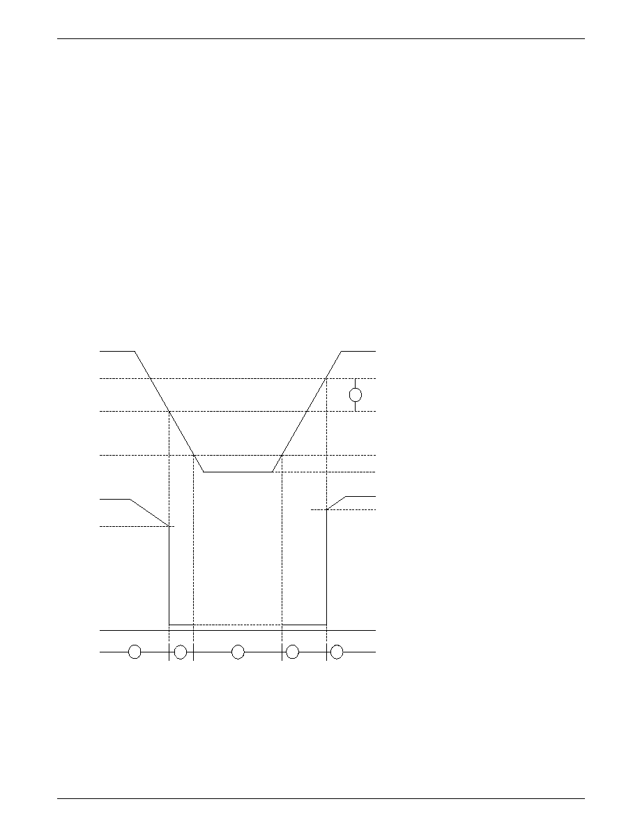
Functional Description
The following designators 1~6 refer to the timing diagram below.
1. While the input voltage (V
IN
) is higher than the detect voltage (V
DF
), the output voltage at V
OUT
pin equals the input volt-
age at V
IN
pin.
2. When the input V
IN
voltage falls lower than V
DF
, V
OUT
drops near ground voltage.
3. If the input voltage decreases below the minimum operating voltage (V
MIN
), the V
OUT
output voltage will be undefined.
4. During an increase of the input voltage from the V
SS
voltage, V
OUT
is undefined at the voltage below V
MIN
. Exceeding the
V
MIN
level, the ouput stays at the ground level (V
SS
) between the minimum operating voltage (V
MIN
) and the detect release
voltage (V
DR
).
5. If the input voltage increases more than V
DR
, the output voltage at V
OUT
pin equals the input voltage at V
IN
pin.
6. The difference between V
DR
and V
DF
is the hysteresis in the system.
ILC5062
PRODUCT SPECIFICATION
4
Rev. 2.2 8/14/02
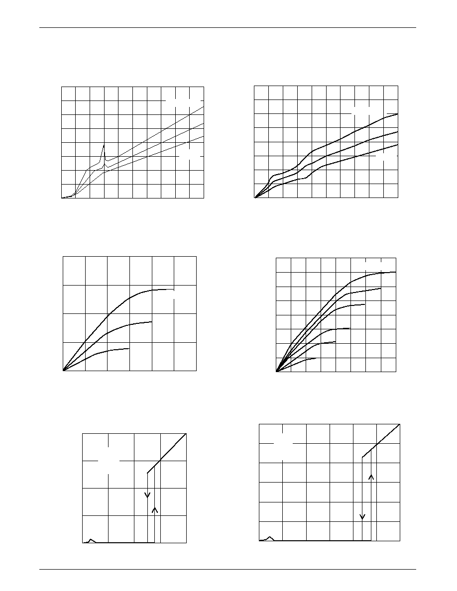
Typical Performance Characteristics -
General conditions for all curves
0
1
2
3
4
ILC5062M-27
Supply Current vs Input Voltage
SUPPLY CURRENT I
SS
(µA)
INPUT VOLTAGE V
IN
(V)
0
1
2
3
4
5
6
7
8
9
10
T
A
= 80∞C
-30∞C
25∞C
0
1
2
3
4
ILC5062M-44
Supply Current vs Input Voltage
SUPPLY CURRENT I
SS
(µA)
INPUT VOLTAGE V
IN
(V)
0
1
2
3
4
T
A
= 80∞C
5
6
7
8
9
10
25∞C
-30∞C
0
0.5
1.0
ILC5062M-27
N-ch Driver Output Current vs V
DS
OUTPUT CURRENT:I
OUT
Nch (mA)
V
DS
(V)
0
10
20
30
40
V
IN
= 2.5V
2.0V
1.5
2.0
2.5
3.0
1.5V
0
1
2
ILC5062M-44
N-ch Driver Output Current vs V
DS
OUTPUT CURRENT:I
OUT
Nch (mA)
V
DS
(V)
0
20
40
60
80
V
IN
= 4.0V
2.0V
3
4
1.5V
10
30
50
70
2.5V
3.5V
3.0V
0
1
2
ILC5062M-27
V
OUT
vs V
IN
OUTPUT VOLTAGE:V
OUT
(V)
INPUT VOLTAGE V
IN
(V)
0
1
2
3
4
3
4
T
A
= 80∞C
25∞C
-30∞C
0
1
2
ILC5062M-44
V
OUT
vs V
IN
OUTPUT VOLTAGE:V
OUT
(V)
INPUT VOLTAGE V
IN
(V)
0
1
2
3
4
3
4
5
6
T
A
= 80∞C
5
6
25∞C
-30∞C

PRODUCT SPECIFICATION
ILC5062
Rev. 2.2 8/14/02
5
Typical Performance Characteristics -
General conditions for all curves
0
1
2
ILC5062M-27
P_ch Driver Output Current vs Input Voltage
OUTPUT CURRENT:I
OUT
pch (mA)
INPUT VOLTAGE V
IN
(V)
0
2
4
6
3
4
5
1.5V
8
10
6
7
8
9
10
1.0V
V
DS
= 2.1V
0.5V
0
1
2
ILC5062M-44
P_ch Driver Output Current vs Input Voltage
OUTPUT CURRENT:IOUTpch (mA)
INPUT VOLTAGE V
IN
(V)
0
2
4
6
3
4
5
8
10
6
7
8
9
10
1.0V
V
DS
= 2.1V
0.5V
12
1.5V
-40
-20
ILC5062M-27
V
DR
and V
DF
vs Temperature
RELEASE VOLTAGE:V
DF
and
RELEASE VOLTAGE:V
DR
AMBIENT TEMPERATURE:T
A
2.5
2.6
2.7
2.8
0
20
2.9
3.0
40
60
80
V
DR
(V)
V
DF
(V)
0
0.5
1.0
ILC5062M-27
N-ch Driver Output Current vs Input Voltage
OUTPUT CURRENT:I
OUT
Nch (mA)
INPUT VOLTAGE V
IN
(V)
0
5
10
15
1.5
2.0
2.5
3.0
V
DS
= 0.5V
20
T
A
= -30∞C
25∞C
80∞C
0
1
2
ILC5062M-44
N-ch Driver Output Current vs Input Voltage
OUTPUT CURRENT:I
OUT
Nch (mA)
INPUT VOLTAGE V
IN
(V)
0
5
10
15
3
4
5
20
25
V
DS
= 0.5V
T
A
= -30∞C
25∞C
80∞C