
www.fairchildsemi.com
Rev. 1.5
©2001 Fairchild Semiconductor Corporation
Features
∑ 85% efficiency at 50mA
∑ Start-up voltages as low as 900mV
∑ ±2.5% accurate outputs
∑ Complete switcher design with only 3 external
components
∑ 50, 100 and 180kHz switching frequency versions
available
∑ Shutdown to 0.5µA Iq
∑ External transistor option allows several hundred
milliamp switcher design
Applications
∑ Cellular Phones, Pagers
∑ Portable Cameras and Video Recorders
∑ Palmtops and PDAs
Description
100mA boost converter in 5-lead SOT-89 package using both
PFM and PWM conversion techniques. In normal operation
the ILC6380 runs in PWM mode running at one of three fixed
frequencies. At light loads the ILC6380 senses when the duty
cycle drops to approximately 10%, and automatically
switches into a power-saving PFM switching technique. This
maintains high efficiencies both at full load and in system
sleep conditions.
Only 3 external components are needed to complete the
switcher design, and standard voltage options of 2.5, 3.3, and
5.0V at ±2.5% accuracy feature on-chip phase compensation
and soft-start design.
ILC6381 drives an external transistor for higher current
switcher design, with all of the features and benefits of the
ILC6380.
Typical Applications
L
V
IN
SD
+
V
OUT
CE
1
3
2
4
5
ILC6380
C
L
GND
L
V
IN
SD
+
V
OUT
CE
1
3
2
4
5
ILC6381
C
L
Tr
GND
R
B
C
B
Figure 1:
L: 100µH (SUMIDA, CD-54)
SD: Diode (Schottky diode; MATSUSHITA MA735)
CL: 16V 47µF (Tantalum Capacitor; NICHICON, F93)
Figure 2:
L: 47µH (SUMIDA, CD-54)
SD: Diode (Schottky diode; MATSUSHITA MA735)
CL: 16V 47µF (Tantalum Capacitor; NICHICON, F93)
RB: 1kW
CB: 3300pF
Tr: 2SC3279, 2SDI628G
ILC6380/81
SOT-89 Step-up Dual-Mode Switcher with Shutdown
©2001 Fairchild Semiconductor Corporation
ILC6380/81
2
©2001 Fairchild Semiconductor Corporation
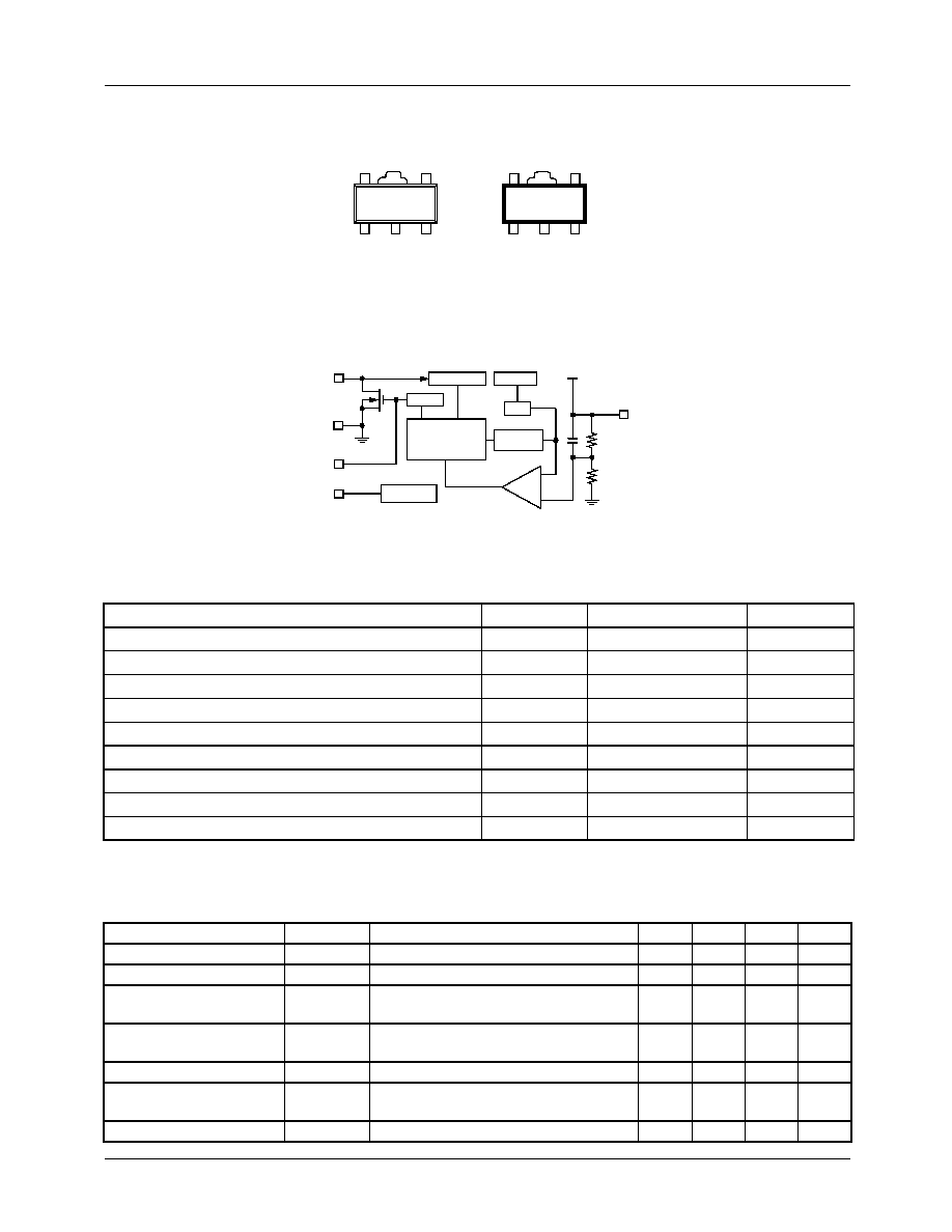
Pin Assignments
Internal Block Diagram
Absolute Maximum Ratings
(T
A
= 25∞C)
Electrical Characteristics
V
OUT
= 5.0V, F
OSC
= 100kHz T
A
- 25∞C. Unless otherwise specified, V
IN
= V
OUT
x 0.6, I
OUT
= 50mA. See schematic, figure 3.
Parameter
Symbol
Ratings
Units
V
OUT
Input Voltage
V
OUT
12
V
Voltage on pin L
X
V
LX
12
V
Current on pin L
X
I
LX
400
mA
Voltage on pin EXT
V
EXT
V
SS
-0.3~V
OUT
+0.3
V
Current on pin EXT
I
EXT
±50
mA
CE Input Voltage
V
CE
12
V
Continuous Total Power Dissipation
P
D
500
mW
Operating Ambient Temperature
T
OPR
-30~+80
∞C
Storage Temperature
T
STG
-40~+125
∞C
Parameter
Symbol
Conditions
Min.
Typ.
Max.
Units
Output Voltage
V
OUT
4.875
5.000
5.125
V
Input Voltage
V
IN
10
V
Oscillation Startup
Voltage
V
ST
L
X
= 10k
pull-up to 5V, V
OUT
= V
ST
0.8
V
Operation Startup
Voltage
V
ST1
I
OUT
= 1mA
0.9
V
No-Load Input Current
I
IN
I
OUT
= 0mA (Note 1)
23.0
46.0
µA
Supply Current 1
(Note 2)
I
DD
1
L
X
= 10k
pull-up to 5V, V
OUT
= 4.5V
78.6
131.1
µA
Supply Current 2
I
DD
2
L
X
= 10k
pull-up to 5V, V
OUT
= 5.5V
6.9
13.8
µA
V
LX
LIMITER
PWM/PFM Controlled
BUFFER
L
X
V
SS
EXT
+
-
CHIP ENABLE
OSC
50/100/180KHz
V
DD
V
OUT
CE
Phase com
V
ref
Slow Start
V
DD
is internally connected to the V
OUT
pin.
SOT -89-5
(TOP VIEW)
1
3
2
V
OUT
CE
L
X
4
5
V
SS
N/C
SOT -89-5
(TOP VIEW)
1
3
2
V
OUT
CE
EXT
4
5
V
SS
N/C
ILC6380
ILC6381

ILC6380/81
3
©2001 Fairchild Semiconductor Corporation
Notes:
1. The Schottky diode (S.D.), in figure 3 must be type MA735, with Reverse current (IR) < 1.0µA at reverse voltage (VR)=10.0V
2. "Supply Current 1" is the supply current while the oscillator is continuously oscillating. In actual operation the oscillator
periodically operates which results in less average power consumption.
The current that is actually provided by external V
IN
source is represented by "No-Load Input Current (I
IN
)"
3. Switching frequency is determined by delay time of internal comparator to turn L
X
"off", and minimum "on" time as determined
by MAXDTY spec.
Electrical Characteristics ILC6380BP-50
V
OUT
= 5.0V, F
OSC
= 100kHz T
A
= 25∞C. Unless otherwise specified, V
IN
= V
OUT
X0.6, I
OUT
= 50mA. See the schematic, figure 4.
L
X
Switch-On Resistance
R
SWON
L
X
= 10k
pull-up to 5V, V
OUT
= 4.5V
1.3
2.3
L
X
Leakage Current
I
LXL
No external components, V
OUT
= VL
X
=
10V
1.0
µA
Oscillator Freq.
F
OSC
L
X
= 10k
pull-up to 5V, V
OUT
= 4.5V,
Measuring of L
X
waveform
85
100
115
kHz
Maximum Duty Ration
MAXDTY
L
X
= 10k
pull-up to 5V, V
OUT
= 4.5V,
Measuring of L
X
on-time
80
87
92
%
PFM Duty Ration
PFMDTY
V
IN
= 4.75V, Measuring of L
X
on-time
5
10
20
%
Stand-by Current
I
STB
L
X
= 10k
pull-up to 5V, V
OUT
= 4.5V
0.5
µA
CE "High" Voltage
V
CEH
L
X
= 10k
pull-up to 5V, V
OUT
= 4.5V,
Existence of L
X
Oscillation
0.75
V
CE "Low" Voltage
V
CEL
L
X
= 10k
pull-up to 5V, V
OUT
= 4.5V,
Stopped L
X
Oscillation
0.20
V
CE "High" Current
I
CEH
L
X
= 10k
pull-up to 5V, V
OUT
= V
CE
=
4.5V
0.25
µA
CE "Low" Current
I
CEL
L
X
= 10k
pull-up to 5V, V
OUT
= 4.5V,
V
CE
= 0V
-0.25
µA
L
X
Limit Voltage
V
LXLMT
L
X
= 10k
pull-up to 5V, V
OUT
= 4.5V,
F
OSC
> F
OSC
x 2 (Note 2)
0.7
1.1
V
Efficiency
EFFI
85
%
Slow Start Time
T
SS
10
msec
Parameter
Symbol
Conditions
Min.
Typ.
Max.
Units
Output Voltage
V
OUT
Test Circuit Figure 2
4.875
5.000
5.125
V
Input Voltage
V
IN
10
V
Oscillation Startup
Voltage
V
ST2
V
OUT
= V
ST2
0.8
V
Operation Startup
Voltage
V
ST1
I
OUT
= 1mA
0.9
V
Supply Current 1
(Note 1)
I
DD
1
EXT = 10k
pull-up 5V,
V
OUT
= 4.5V
78.6
131.1
µA
Supply Current 2
I
DD
2
EXT = 10k
pull-up 5V,
V
OUT
= 5.5V
6.9
13.8
µA
EXT "High" On-
Resistance
R
EXTH
EXT
= 10k
pull-up to 5V,
V
OUT
= 4.5V, V
EXT
= V
OUT
- 0.4V
30
50
Parameter
Symbol
Conditions
Min.
Typ.
Max.
Units
Electrical Characteristics (continued)

ILC6380/81
4
©2001 Fairchild Semiconductor Corporation
EXT "Low" On-
Resistance
R
EXTL
EXT
= 10k
pull-up to 5V,
V
OUT
= 4.5V, V
EXT
= V
OUT
- 0.4V
30
50
Oscillator Frequency
F
OSC
EXT
= 10k
pull-up to 5V,
V
OUT
= 4.5V, Measuring of EXT
waveform
85
100
115
kHz
Maximum Duty Ratio
MAXDTY EXT
= 10k
pull-up to 5V,
V
OUT
= 4.5V, Measuring of EXT high
state
80
87
92
%
CE "High" Voltage
V
CEH
EXT
= 10k
pull-up to 5V,
V
OUT
= 4.5V, Existence of Oscillation
0.75
V
CE "Low" Voltage
V
CEL
EXT
= 10k
pull-up to 5V,
V
OUT
= 4.5V, Stopped EXT Oscillation
0.20
V
CE "High" Current
I
CEH
EXT
= 10k
pull-up to 5V,
V
OUT
= 4.5V, V
CE
= V
OUT
x 0.95V
0.25
µA
CE "Low" Current
I
CEL
EXT
= 10k
pull-up to 5V,
V
OUT
= 4.5V, V
CE
= 0V
-0.25
µA
Efficiency
EFFI
85
%
Slow Start Time
T
SS
10
msec
Parameter
Symbol
Conditions
Min.
Typ.
Max.
Units
Electrical Characteristics ILC6380BP-50 (continued)
Notes:
1. The Schottky diode (S.D.), in figure 3 must be type MA735, with Reverse current (IR) < 1.0µA at reverse voltage
(VR)=10.0V
2. "Supply Current 1" is the supply current while the oscillator is continuously oscillating. In actual operation the oscillator
periodically operates which results in less average power consumption.
The current that is actually provided by external V
IN
source is represented by "No-Load Input Current (I
IN
)"

ILC6380/81
5
©2001 Fairchild Semiconductor Corporation
Functions and Operation
The ILC6380 performs boost DC-DC conversion by control-
ling the switch element shown in the circuit below
When the switch is closed, current is built up through the
inductor. When the switch opens, this current has to go
somewhere and is forced through the diode to the output. As
this on and off switching continues, the output capacitor
voltage builds up due to the charge it is storing from the
inductor current. In this way, the output voltage gets boosted
relative to the input. The ILC6380 monitors the voltage on
the output capacitor to determine how much and how often
to drive the switch.
In general, the switching characteristic is determined by the
output voltage desired and the current required by the load.
Specifically the energy transfer is determined by the power
stored in the coil during each switching cycle.
PL = (t
ON
, V
IN
)
The ILC6380 and ILC6381 use a PWM or Pulse Width
Modulation technique. The parts come in one of three fixed
internal frequencies: 50, 100, or 180kHz. The switches are
constantly driven at these frequencies. The control circuitry
varies the power being delivered to the load by varying the
on-time, or duty cycle, of the switch. Since more on-time
translates to higher current build-up in the inductor, the max-
imum duty cycle of the switch determines the maximum load
current that the device can support. The ILC6380 and
ILC6381 both support up to 87% duty cycles, for maximum
usable range of load currents.
There are two key advantages of the PWM type controllers.
First, because the controller automatically varies the duty
cycle of the switch's on-time in response to changing load
conditions, the PWM controller will always have an opti-
mized waveform for a steady-state load. This translates to
very good efficiency at high currents and minimal ripple on
the output. [Ripple is due to the output cap constantly
accepting and storing the charge received from the inductor,
and delivering charge as required by the load. The "pump-
ing" action of the switch produces a sawtooth-shaped volt-
age as seen by the output.]
The other key advantage of the PWM type controllers is that
the radiated noise due to the switching transients will always
occur at the (fixed) switching frequency. Many applications
do not care much about switching noise, but certain types of
applications, especially communication equipment, need to
minimize the high frequency interference within their system
as much as is possible. Using a boost converter requires a
certain amount of higher frequency noise to be generated;
using a PWM converter makes that noise highly predictable;
thus easier to filter out.
Dual Mode Operation
But there are downsides of PWM approaches, especially at
very low currents. Because the PWM technique relies on
constant switching and varying duty cycle to match the load
conditions, there is some point where the load current gets
too small to be handled efficiently. An actual switch con-
sumes some finite amount of current to switch on and off; at
very low currents this can be of the same magnitude as the
load current itself, driving switching efficiencies down to
50% and below. The ILC6380 and ILC6381 overcome this
limitation by automatically switching over to a PFM, or
Pulse Frequency Modulation, technique at low currents. This
technique conserves power loss by only switching the output
if the current drain requires it. As shown in the diagram
below, the waveform actually skips pulses depending on the
power needed by the output. [This technique is also called
"pulse skipping" because of this characteristic.]
In the ILC6380 and ILC6381, this switchover is internally
set to be at the point where the PWM waveform hits
approximately 10% duty cycle. So the PFM mode is running
at 10% duty cycle at the rated frequency; for 100kHz part
this means a constant on-time of 1msec. This not only is
ideal for efficiency at these low currents, but a 10% duty
cycle will have much better output ripple characteristics than
a similarly configured PFM part, such as the ILC6390 and
ILC6391.
The Dual-Mode architecture was designed specifically for
those applications, like communications, which need the
spectral predictability of a PWM-type DC-DC converter, yet
which also needs the highest efficiencies possible, especially
in Shutdown or Standby mode. [For other conversion
techniques, please see the ILC6370/71 and ILC6390/91
datasheets.]
Other Considerations
The other limitation of PWM techniques is that, while the
fundamental switching frequency is easier to filter out since
it's constant, the higher order harmonics of PWM will be
present and may have to be filtered out, as well. Any filtering
V
S E T
V
O U T
Switch
W a v e f o r m