www.fairchildsemi.com
REV. 1.0.5 3/21/02
Features
∑ 1% output voltage accuracy
∑ Low noise
∑ Only 75µA ground current at 80mA load
∑ Ripple rejection up to 75dB at 1kHz
∑ Excellent line and load transient response
∑ Guaranteed to 80mA output current
∑ Industry standard five lead SC70 packages
∑ Fixed 2.5V, 2.6V, 2.7V, 2.8V, 2.85V, 2.9V, 3.0V, 3.1V,
3.3V and custom output voltage options
Applications
∑ Cellular phones
∑ Wireless communicators
∑ PDAs / palmtops / organizers
∑ Battery powered portable electronics
General Description
The ILC7010/7011 is an 80mA, Ultra Low Noise, Low
Dropout (LDO) linear regulator, designed and processed in
CMOS technology. This process combines the best CMOS
features of low quiescent current, small size and low dropout
voltage with the best bipolar features of high ripple rejection,
ultra low noise and power handling capability. The ILC7010/
7011 offers a quiescent current of less than 100
µ
A, a logic
level enable (regulator EN) pin, a footprint that is half the
size of the industry standard SOT-23, and a low dropout
voltage of 25mV at 10mA. With better than 70 dB (1kHz) of
ripple rejection, low noise of 40µV RMS and 1% output
voltage accuracy, the ILC7010/7011 sets a new standard in
linear regulators for communications and personal
electronics applications.
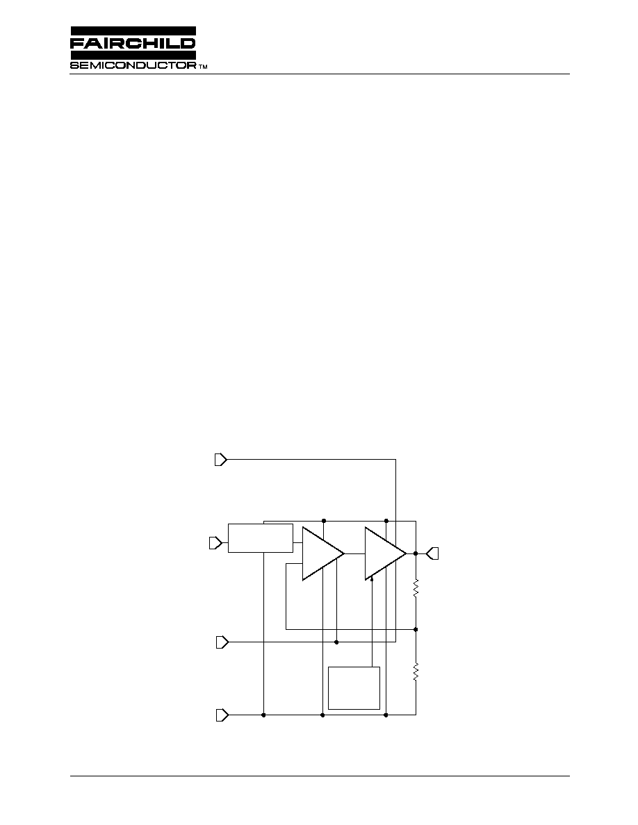
Block Diagram
V
IN
CN
(ILC7011
only)
EN
+
≠
GND
V
OUT
Error
Amplifier
Voltage
Reference
Thermal
Shut
Down
Trans-
conductance
Amplifier
ILC7010/7011
80mA SC70 Low Noise CMOS RF-LDOTM Regulator
ILC7010/7011
PRODUCT SPECIFICATION
2
REV. 1.0.5 3/21/02
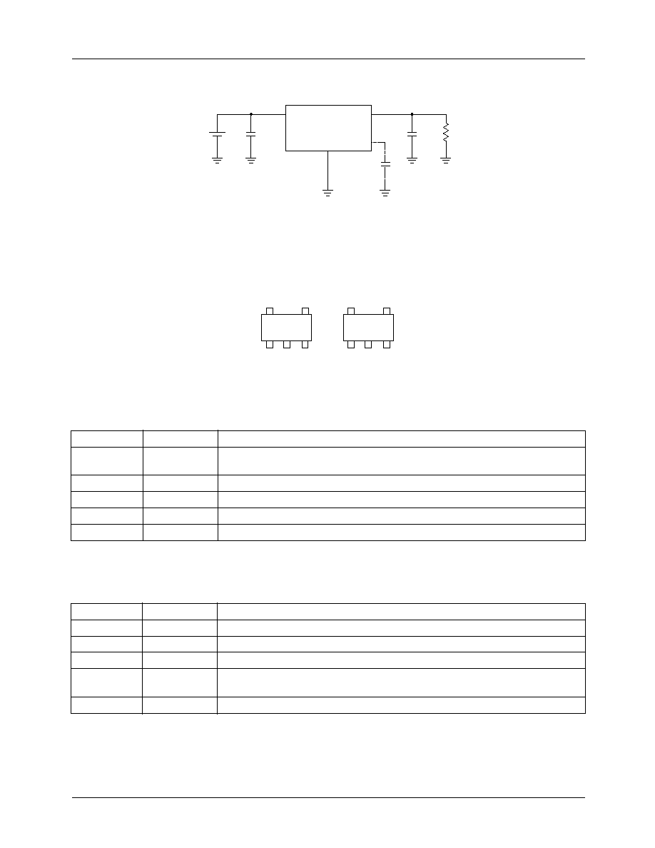
Test circuit
Figure 1.
Pin Configuration
Pin Definition ILC7010
Pin Definition ILC7011
Pin Number
Pin Name
Pin Function Description
1
EN
Enable input
. High level enables V
OUT
while Low level commands shutdown
mode and discharge C
OUT
to GND
2
N/C
Not connected
3
GND
Ground of the IC
4
V
OUT
Voltage output
. Regulated output voltage
5
V
IN
Supply voltage input
Pin Number
Pin Name
Pin Function Description
1
V
OUT
Voltage output
. Regulated output voltage
2
GND
Ground of the IC
3
V
IN
Supply voltage input
4
EN
Enable input
. High level enables V
OUT
while Low level commands shutdown
mode and discharge C
OUT
to GND
5
CN
Optional noise bypass capacitor
V
IN
C
IN
C
N
C
OUT
R
L
V
IN
EN
V
OUT
(CN)
GND
V
IN
1
2
3
1
2
3
5
4
5
4
V
OUT
EN N/C GND
ILC7010
V
IN
V
OUT
EN
CN
SC70
GND
ILC7011
PRODUCT SPECIFICATION
ILC7010/7011
REV. 1.0.5 3/21/02
3
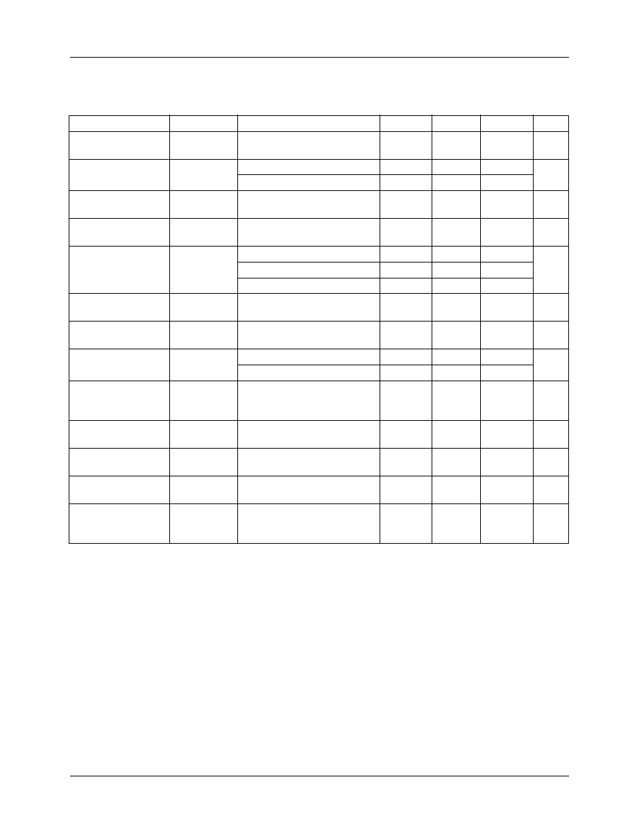
Absolute Maximum Ratings
Absolute maximum ratings are the values beyond which the device may be damaged or have its useful life
impaired. Functional operation under these conditions is not implied.
Recommended Operating Conditions
Parameter
Min.
Max.
Units
Supply Voltage
10
V
EN Input Voltage
-0.3
V
IN
+ 0.3
V
Output Voltage
-0.3
V
IN
+ 0.3
V
Junction Temperature (T
J
)
150, Internally limited
∞C
Storage Temperature
-40
150
∞C
Lead Soldering Temperature, 10 seconds
300
∞C
Power Dissipation (P
D
)
150
mW
Parameter
Conditions
Min.
Typ.
Max.
Units
Supply Voltage V
DD
V
IN
to GND
V
OUT
+V
DO
V
OUT
+1
V
OUT
+4
V
Peak Output Current
I
OUT
to GND,
tpw=2mS
120
mA
Ambient Operating Temperature
T
A
-40
85
∞
C
ILC7010/7011
PRODUCT SPECIFICATION
4
REV. 1.0.5 3/21/02
Electrical Specifications
V
IN
=V
OUT
+1V, I
OUT
=1mA, V
EN
=2V and T
A
= +25∞C using circuit in Figure 1 with C
IN
=C
OUT
=1µF, C
N
=0,
unless otherwise specified
Notes:
1. For 2.5V < V
OUT
< 2.8V refer to diagram "Dropout Voltage vs. Output Voltage."
2. Dropout voltage is defined as the input to output differential voltage at which the output voltage drops 2% below the nominal
value measured with 1V differential.
Parameter
Symbol
Conditions
Min.
Typ.
Max.
Units
Output Voltage
V
OUT
0.99
V
OUTnom
V
OUTnom
1.01
V
OUTnom
V
Ground pin Current
I
GND
I
OUT
=10mA
70
90
µ
A
I
OUT
=80mA
90
110
Line Regulation
V
OUT
/
V
OUT
/
V
IN
V
IN
: V
OUT
+1V to V
OUT
+2V
0.017
0.075
%/V
Load
Regulation
V
OUT
/
V
OUT
I
OUT
=1 to 80mA
0.12
0.2
%
Dropout Voltage
1,2
V
DO
I
OUT
=10mA, V
OUT
>2.8V
25
30
mV
I
OUT
=20mA, V
OUT
>2.8V
50
60
I
OUT
=80mA, V
OUT
>2.8V
220
250
Shutdown
(OFF) current
I
OFF
V
EN
=0
10
40
nA
EN Input Voltage
V
EN
High = ON state
Low = OFF state
2
0.6
V
EN Input Current
I
EN
V
EN
=0.6V
0.3
µ
A
V
EN
=2V
1
Output Noise
Voltage ILC7011
eN
BW=300Hz to 50kHz
C
IN
=C
OUT
=2.2uF, C
N
=10nF
I
OUT
=10mA
40
µ
V
RMS
Ripple Rejection
PSRR
C
OUT
=4.7uF, 120Hz
I
OUT
=80mA
65
dB
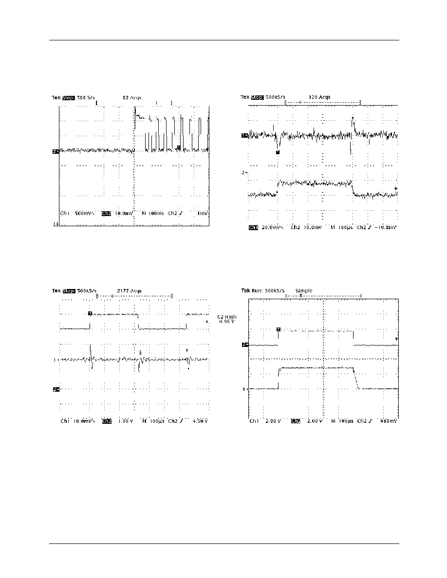
Dynamic Line
Regulation
V
OUT
(line)
V
IN
=1V,I
OUT
=80mA,
tr/tf=2uS
10
mV
Dynamic Load
Regulation
V
OUT
(load)
I
OUT
=80mA, tr<5mS
15
mV
Resistance
Discharge in OFF
state
R
DISC
V
EN
=0
1.5
k