 | –≠–ª–µ–∫—Ç—Ä–æ–Ω–Ω—ã–π –∫–æ–º–ø–æ–Ω–µ–Ω—Ç: IRF510A | –°–∫–∞—á–∞—Ç—å:  PDF PDF  ZIP ZIP |
IRF510A
BV
DSS
= 100 V
R
DS(on)
= 0.4
I
D
= 5.6 A
100
5.6
4
20
±
20
63
5.6
3.3
6.5
33
0.22
- 55 to +175
300
4.51
--
62.5
--
0.5
--
n
Avalanche Rugged Technology
n
Rugged Gate Oxide Technology
n
Lower Input Capacitance
n
Improved Gate Charge
n
Extended Safe Operating Area
n
175
∞
C Operating Temperature
n
Lower Leakage Current : 10
A (Max.) @ V
DS
= 100V
n
Lower R
DS(ON)
: 0.289
(Typ.)
Advanced Power MOSFET
Thermal Resistance
Junction-to-Case
Case-to-Sink
Junction-to-Ambient
R
JC
R
CS
R
JA
∞
C/W
Characteristic
Max.
Units
Symbol
Typ.
FEATURES
Absolute Maximum Ratings
Drain-to-Source Voltage
Continuous Drain Current (T
C
=25
)
Continuous Drain Current (T
C
=100
)
Drain Current-Pulsed
(1)
Gate-to-Source Voltage
Single Pulsed Avalanche Energy
(2)
Avalanche Current
(1)
Repetitive Avalanche Energy
(1)
Peak Diode Recovery dv/dt (2)
Total Power Dissipation (T
C
=25
)
Linear Derating Factor
Operating Junction and
Storage Temperature Range
Maximum Lead Temp. for Soldering
Purposes, 1/8? from case for 5-seconds
Characteristic
Value
Units
Symbol
I
DM
V
GS
E
AS
I
AR
E
AR
dv/dt
I
D
P
D
T
J
, T
STG
T
L
A
V
mJ
A
mJ
V/ns
W
W/
∞
C
A
∞
C
V
DSS
V
TO-220
1.Gate 2. Drain 3. Source
3
2
1
Rev. B1
IRF510A
100
--
2.0
--
--
--
--
--
0.11
--
--
--
--
--
55
21
10
14
28
18
8.5
1.6
4.1
--
--
4.0
100
-100
10
100
0.4
--
240
65
25
30
40
70
50
12
--
--
3.49
190
--
--
--
85
0.23
5.6
20
1.5
--
--
Notes ;
(1) Repetitive Rating : Pulse Width Limited by Maximum Junction Temperature
(2) L=3mH, I
AS
=5.6A, V
DD
=25V, R
G
=27
, Starting T
J
=25
∞
C
(3) I
SD
5.6A, di/dt
250A/
s, V
DD
BV
DSS
, Starting T
J
=25
∞
C
(4) Pulse Test : Pulse Width = 250
µ
s, Duty Cycle
2%
(5) Essentially Independent of Operating Temperature
N-CHANNEL
POWER MOSFET
Electrical Characteristics
(T
C
=25
∞
C unless otherwise specified)
Drain-Source Breakdown Voltage
Breakdown Voltage Temp. Coeff.
Gate Threshold Voltage
Gate-Source Leakage , Forward
Gate-Source Leakage , Reverse
Characteristic
Symbol
Max. Units
Typ.
Min.
Test Condition
Static Drain-Source
On-State Resistance
Forward Transconductance
Input Capacitance
Output Capacitance
Reverse Transfer Capacitance
Turn-On Delay Time
Rise Time
Turn-Off Delay Time
Fall Time
Total Gate Charge
Gate-Source Charge
Gate-Drain ("Miller") Charge
g
fs
C
iss
C
oss
C
rss
t
d(on)
t
r
t
d(off)
t
f
Q
g
Q
gs
Q
gd
BV
DSS
BV/
T
J
V
GS(th)
R
DS(on)
I
GSS
I
DSS
V
V/
∞
C
V
nA
A
S
pF
ns
nC
--
--
--
--
--
--
--
--
--
--
--
--
--
V
GS
=0V,I
D
=250
µ
A
I
D
=250
µ
A See Fig 7
V
DS
=5V,I
D
=250
µ
A
V
GS
=20V
V
GS
=-20V
V
DS
=100V
V
DS
=80V,T
C
=150
∞
C
V
GS
=10V,I
D
=2.8A
(4)
V
DS
=40V,I
D
=2.8A
(4)
V
DD
=50V,I
D
=5.6A,
R
G
=24
See Fig 13 (4)(5)
V
DS
=80V,V
GS
=10V,
I
D
=5.6A
See Fig 6 & Fig 12 (4)(5)
Drain-to-Source Leakage Current
V
GS
=0V,V
DS
=25V,f =1MHz
See Fig 5
Source-Drain Diode Ratings and Characteristics
Continuous Source Current
Pulsed-Source Current (1)
Diode Forward Voltage
(4)
Reverse Recovery Time
Reverse Recovery Charge
I
S
I
SM
V
SD
t
rr
Q
rr
Characteristic
Symbol
Max. Units
Typ.
Min.
Test Condition
--
--
--
--
--
A
V
ns
µ
C
Integral reverse pn-diode
in the MOSFET
T
J
=25
∞
C,I
S
=5.6A,V
GS
=0V
T
J
=25
∞
C,I
F
=5.6A
di
F
/dt=100A/
µ
s
(4)
IRF510A
10
-1
10
0
10
1
10
-1
10
0
10
1
@ Notes :
1. 250
µ
s Pulse Test
2. T
C
= 25
o
C
V
GS
Top : 1 5 V
1 0 V
8.0 V
7.0 V
6.0 V
5.5 V
5.0 V
Bottom : 4.5 V
I
D
, Dr
ai
n Cu
rr
en
t [A
]
V
DS
, Drain-Source Voltage [V]
2
4
6
8
10
10
-1
10
0
10
1
25
o
C
175
o
C
- 55
o
C
@ Notes :
1. V
GS
= 0 V
2. V
DS
= 40 V
3. 250
µ
s Pulse Test
I
D
,
Drain
Curr
ent
[A]
V
GS
, Gate-Source Voltage [V]
0
5
10
15
20
0.0
0.2
0.4
0.6
0.8
@ Note : T
J
= 25
o
C
V
GS
= 20 V
V
GS
= 10 V
R
DS
(o
n)
, [
]
Dr
ai
n-
So
ur
ce
O
n
-
Res
is
ta
nc
e
I
D
, Drain Current [A]
0.4
0.6
0.8
1.0
1.2
1.4
1.6
1.8
2.0
10
-1
10
0
10
1
175
o
C
25
o
C
@ Notes :
1. V
GS
= 0 V
2. 250
µ
s Pulse Test
I
DR
,
Rever
se Dr
ain C
urren
t [A
]
V
SD
, Source-Drain Voltage [V]
10
0
10
1
0
70
140
210
280
350
C
iss
= C
gs
+ C
gd
(
C
ds
= shorted
)
C
oss
= C
ds
+ C
gd
C
rss
= C
gd
@ Notes :
1. V
GS
= 0 V
2. f = 1 MHz
C
rss
C
oss
C
iss
Ca
pa
ci
ta
nc
e
[
p
F
]
V
DS
, Drain-Source Voltage [V]
0
2
4
6
8
10
0
5
10
V
DS
= 80 V
V
DS
= 50 V
V
DS
= 20 V
@ Notes : I
D
= 5.6 A
V
GS
,
Gate-
Sourc
e Vol
tage
[V]
Q
G
, Total Gate Charge [nC]
N-CHANNEL
POWER MOSFET
Fig 1. Output Characteristics
Fig 2. Transfer Characteristics
Fig 6. Gate Charge vs. Gate-Source Voltage
Fig 5. Capacitance vs. Drain-Source Voltage
Fig 4. Source-Drain Diode Forward Voltage
Fig 3. On-Resistance vs. Drain Current
IRF510A
-75
-50
-25
0
25
50
75
100
125
150
175
200
0.8
0.9
1.0
1.1
1.2
@ Notes :
1. V
GS
= 0 V
2. I
D
= 250
µ
A
BV
DS
S
,
(
Nor
mal
iz
ed)
Dr
ai
n-S
our
ce
Br
ea
kdo
wn
Vo
lta
ge
T
J
, Junction Temperature [
o
C]
-75
-50
-25
0
25
50
75
100
125
150
175
200
0.0
0.5
1.0
1.5
2.0
2.5
3.0
@ Notes :
1. V
GS
= 10 V
2. I
D
= 2.8 A
R
DS
(o
n)
,
(No
rma
liz
ed)
Dr
ain-
Sou
rce
On-
Res
ist
ance
T
J
, Junction Temperature [
o
C]
10
0
10
1
10
2
10
-1
10
0
10
1
10
2
DC
100
µ
s
1 ms
10 ms
@ Notes :
1. T
C
= 25
o
C
2. T
J
= 175
o
C
3. Single Pulse
Operation in This Area
is Limited by R
DS(on)
I
D
,
D
rai
n C
u
r
ren
t
[A
]
V
DS
, Drain-Source Voltage [V]
10
- 5
10
- 4
10
- 3
10
- 2
10
- 1
10
0
10
1
10
- 1
10
0
single pulse
0.2
0.1
0.01
0.02
0.05
D=0.5
@ Notes :
1. Z
J C
(t)=4.51
o
C/W Max.
2. Duty Factor, D=t
1
/t
2
3. T
J M
-T
C
=P
D M
*Z
J C
(t)
Z
JC
(t)
,
Therm
al R
espon
se
t
1
, Square Wave Pulse Duration [sec]
25
50
75
100
125
150
175
0
1
2
3
4
5
6
I
D
,
Drai
n Cur
rent
[A
]
T
c
, Case Temperature [
o
C]
N-CHANNEL
POWER MOSFET
Fig 7. Breakdown Voltage vs. Temperature
Fig 8. On-Resistance vs. Temperature
Fig 11. Thermal Response
Fig 10. Max. Drain Current vs. Case Temperature
Fig 9. Max. Safe Operating Area
P
DM
t
1
t
2
IRF510A
N-CHANNEL
POWER MOSFET
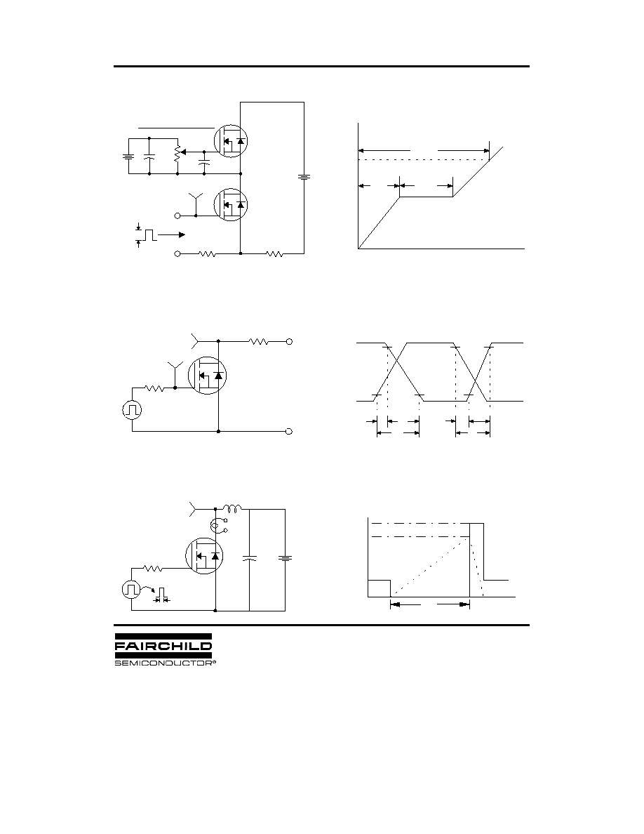
Fig 12. Gate Charge Test Circuit & Waveform
Fig 13. Resistive Switching Test Circuit & Waveforms
Fig 14. Unclamped Inductive Switching Test Circuit & Waveforms
E
AS
=
L
L
I
AS
2
----
2
1
--------------------
BV
DSS
-- V
DD
BV
DSS
V
in
V
out
10%
90%
t
d(on)
t
r
t
on
t
off
t
d(off)
t
f
Charge
V
GS
10V
Q
g
Q
gs
Q
gd
Vary t
p
to obtain
required peak I
D
10V
V
DD
C
L
L
V
DS
I
D
R
G
t
p
DUT
BV
DSS
t
p
V
DD
I
AS
V
DS
(t)
I
D
(t)
Time
V
DD
( 0.5 rated V
DS
)
10V
V
out
V
in
R
L
DUT
R
G
3mA
V
GS
Current Sampling (I
G
)
Resistor
Current Sampling (I
D
)
Resistor
DUT
V
DS
300nF
50K
200nF
12V
Same Type
as DUT
* Current Regulator "
R
1
R
2
IRF510A
N-CHANNEL
POWER MOSFET
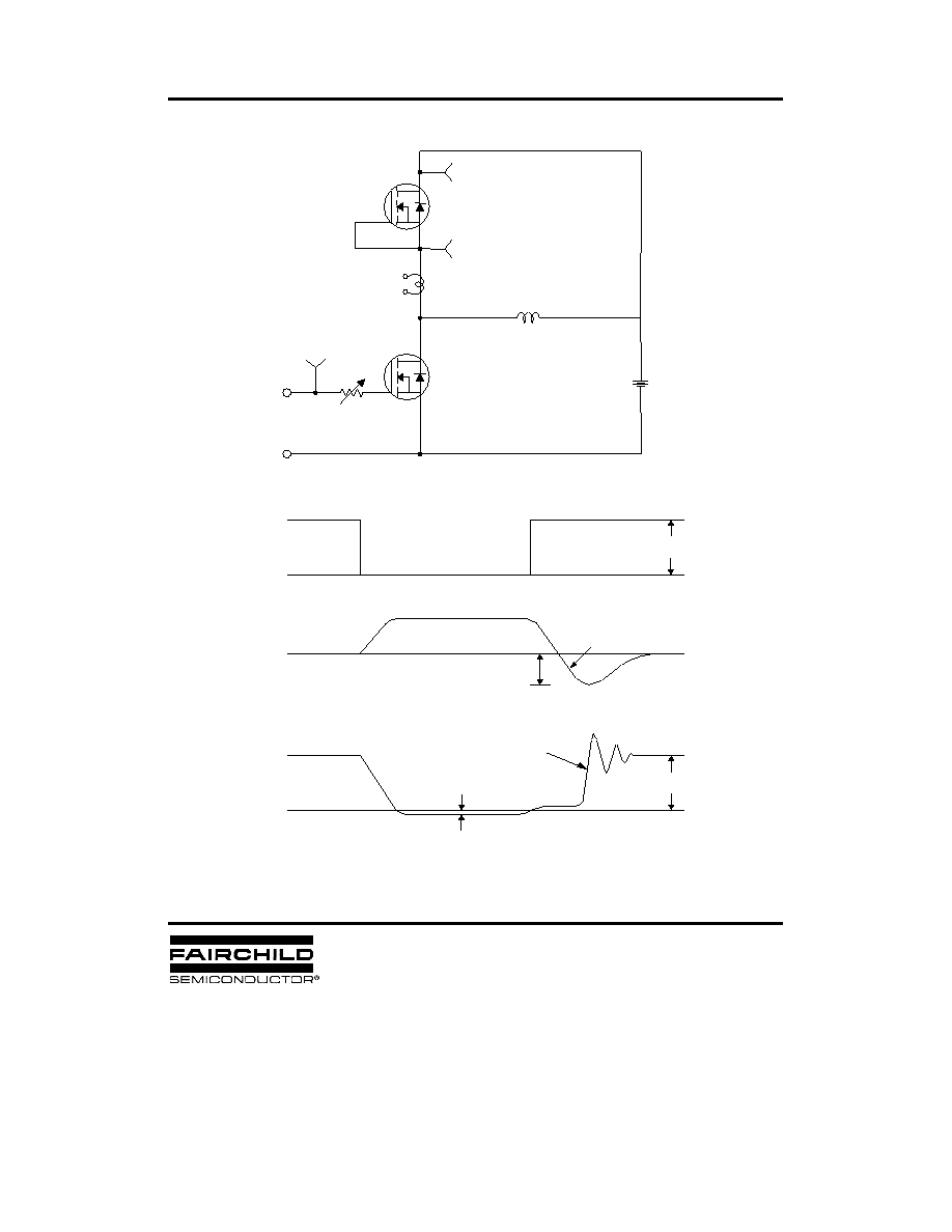
Fig 15. Peak Diode Recovery dv/dt Test Circuit & Waveforms
DUT
V
DS
+
--
L
I
S
Driver
V
GS
R
G
Same Type
as DUT
V
GS
∑ dv/dt controlled by "R
G
"
∑ I
S
controlled by Duty Factor "D"
V
DD
10V
V
GS
( Driver )
I
S
( DUT )
V
DS
( DUT )
V
DD
Body Diode
Forward Voltage Drop
V
f
I
FM
, Body Diode Forward Current
Body Diode Reverse Current
I
RM
Body Diode Recovery dv/dt
di/dt
D =
Gate Pulse Width
Gate Pulse Period
--------------------------

DISCLAIMER
FAIRCHILD SEMICONDUCTOR RESERVES THE RIGHT TO MAKE CHANGES WITHOUT FURTHER
NOTICE TO ANY PRODUCTS HEREIN TO IMPROVE RELIABILITY, FUNCTION OR DESIGN. FAIRCHILD
DOES NOT ASSUME ANY LIABILITY ARISING OUT OF THE APPLICATION OR USE OF ANY PRODUCT
OR CIRCUIT DESCRIBED HEREIN; NEITHER DOES IT CONVEY ANY LICENSE UNDER ITS PATENT
RIGHTS, NOR THE RIGHTS OF OTHERS.
TRADEMARKS
The following are registered and unregistered trademarks Fairchild Semiconductor owns or is authorized to use and is
not intended to be an exhaustive list of all such trademarks.
LIFE SUPPORT POLICY
FAIRCHILDS PRODUCTS ARE NOT AUTHORIZED FOR USE AS CRITICAL COMPONENTS IN LIFE SUPPORT
DEVICES OR SYSTEMS WITHOUT THE EXPRESS WRITTEN APPROVAL OF FAIRCHILD SEMICONDUCTOR CORPORATION.
As used herein:
1. Life support devices or systems are devices or
systems which, (a) are intended for surgical implant into
the body, or (b) support or sustain life, or (c) whose
failure to perform when properly used in accordance
with instructions for use provided in the labeling, can be
reasonably expected to result in significant injury to the
user.
2. A critical component is any component of a life
support device or system whose failure to perform can
be reasonably expected to cause the failure of the life
support device or system, or to affect its safety or
effectiveness.
PRODUCT STATUS DEFINITIONS
Definition of Terms
Datasheet Identification
Product Status
Definition
Advance Information
Preliminary
No Identification Needed
Obsolete
This datasheet contains the design specifications for
product development. Specifications may change in
any manner without notice.
This datasheet contains preliminary data, and
supplementary data will be published at a later date.
Fairchild Semiconductor reserves the right to make
changes at any time without notice in order to improve
design.
This datasheet contains final specifications. Fairchild
Semiconductor reserves the right to make changes at
any time without notice in order to improve design.
This datasheet contains specifications on a product
that has been discontinued by Fairchild semiconductor.
The datasheet is printed for reference information only.
Formative or
In Design
First Production
Full Production
Not In Production
MICROWIRE
OPTOLOGIC
OPTOPLANAR
PACMAN
POP
Power247
PowerTrench
QFET
QS
QT Optoelectronics
Quiet Series
FAST
FASTr
FRFET
GlobalOptoisolator
GTO
HiSeC
I
2
C
ISOPLANAR
LittleFET
MicroFET
MicroPak
Rev. H5
‚
ACEx
Bottomless
CoolFET
CROSSVOLT
DenseTrench
DOME
EcoSPARK
E
2
CMOS
TM
EnSigna
TM
FACT
FACT Quiet Series
SILENT SWITCHER
SMART START
SPM
STAR*POWER
Stealth
SuperSOT-3
SuperSOT-6
SuperSOT-8
SyncFET
TinyLogic
TruTranslation
‚
‚
‚
STAR*POWER is used under license
UHC
UltraFET
VCX
‚