Äîêóìåíòàöèÿ è îïèñàíèÿ www.docs.chipfind.ru
©2002 Fairchild Semiconductor Corporation
January 2002
Rev. B, January 2002
ISL9N312AP3/ISL9N312AS3ST
ISL9N312AP3/ISL9N312AS3ST
N-Channel Logic Level PWM Optimized UltraFET® Trench Power MOSFETs
General Description
This device employs a new advanced trench MOSFET
technology and features low gate charge while maintaining
low on-resistance.
Optimized for switching applications, this device improves
the overall efficiency of DC/DC converters and allows
operation to higher switching frequencies.
Applications
· DC/DC converters
Features
· Fast switching
· r
DS(ON)
= 0.010
(Typ), V
GS
= 10V
· r
DS(ON)
= 0.017
(Typ), V
GS
= 4.5V
· Q
g
(Typ) = 13nC, V
GS
= 5V
· Q
gd
(Typ) = 4.5nC
· C
ISS
(Typ) = 1450pF
MOSFET Maximum Ratings
T
A
= 25°C unless otherwise noted
Thermal Characteristics
Package Marking and Ordering Information
Symbol
Parameter
Ratings
Units
V
DSS
Drain to Source Voltage
30
V
V
GS
Gate to Source Voltage
±
20
V
I
D
Drain Current
58
A
Continuous (T
C
= 25
o
C, V
GS
= 10V)
Continuous (T
C
= 100
o
C, V
GS
= 4.5V)
32
A
Continuous (T
C
= 25
o
C, V
GS
= 10V, R
JA
= 43
o
C/W)
12
A
Pulsed
Figure 4
A
P
D
Power dissipation
Derate above 25
o
C
75
0.5
W
W/
o
C
T
J
, T
STG
Operating and Storage Temperature
-55 to 175
o
C
R
JC
Thermal Resistance Junction to Case TO-220, TO-263
2
o
C/W
R
JA
Thermal Resistance Junction to Ambient TO-220, TO-263
62
o
C/W
R
JA
Thermal Resistance Junction to Ambient TO-263, 1in
2
copper pad area
43
o
C/W
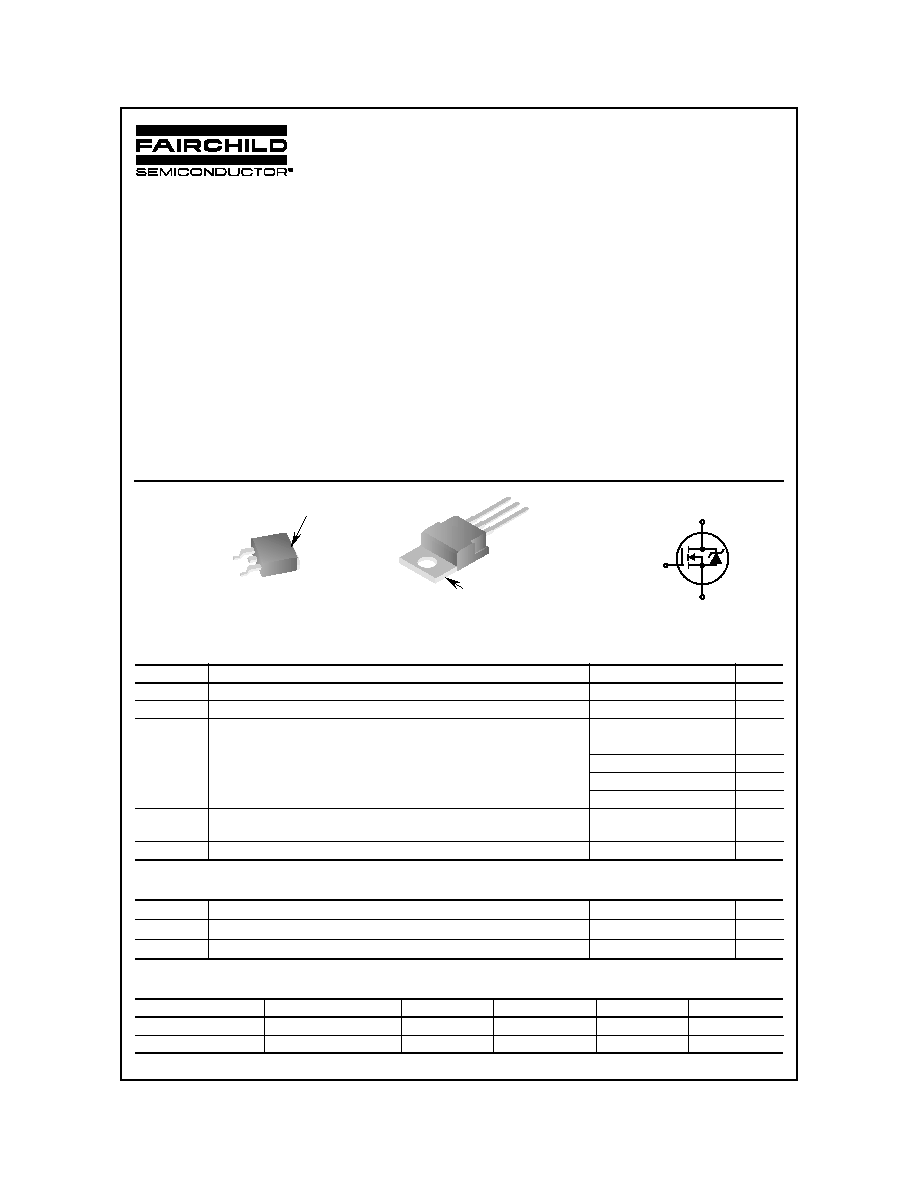
Device Marking
Device
Package
Reel Size
Tape Width
Quantity
N312AS
ISL9N312AS3ST
TO-263AB
330mm
24mm
800 units
N312AP
ISL9N312AP3
TO-220AB
Tube
N/A
50
D
G
S
TO-263AB
TO-220AB
GATE
SOURCE
DRAIN
(FLANGE)
DRAIN
(FLANGE)
DRAIN
SOURCE
GATE
©2002 Fairchild Semiconductor Corporation
Rev. B, January 2002
ISL9N312AP3/ISL9N312AS3ST
Electrical Characteristics
T
A
= 25°C unless otherwise noted
Off Characteristics
On Characteristics
Dynamic Characteristics
Switching Characteristics
(V
GS
= 4.5V)
Switching Characteristics
(V
GS
= 10V)
Unclamped Inductive Switching
Drain-Source Diode Characteristics
Symbol
Parameter
Test Conditions
Min
Typ
Max
Units
B
VDSS
Drain to Source Breakdown Voltage
I
D
= 250
µ
A, V
GS
= 0V
30
-
-
V
I
DSS
Zero Gate Voltage Drain Current
V
DS
= 25V
-
-
1
µ
A
V
GS
= 0V
T
C
= 150
o
-
-
250
I
GSS
Gate to Source Leakage Current
V
GS
=
±
20V
-
-
±
100
nA
V
GS(TH)
Gate to Source Threshold Voltage
V
GS
= V
DS
, I
D
= 250
µ
A
1
-
3
V
r
DS(ON)
Drain to Source On Resistance
I
D
= 58A, V
GS
= 10V
-
0.010
0.012
I
D
= 32A, V
GS
= 4.5V
-
0.017
0.020
C
ISS
Input Capacitance
V
DS
= 15V, V
GS
= 0V,
f = 1MHz
-
1450
-
pF
C
OSS
Output Capacitance
-
300
-
pF
C
RSS
Reverse Transfer Capacitance
-
120
-
pF
Q
g(TOT)
Total Gate Charge at 10V
V
GS
= 0V to 10V
V
DD
= 15V
I
D
= 32A
I
g
= 1.0mA
25
38
nC
Q
g(5)
Total Gate Charge at 5V
V
GS
= 0V to 5V
-
13
20
nC
Q
g(TH)
Threshold Gate Charge
V
GS
= 0V to 1V
-
1.5
2.3
nC
Q
gs
Gate to Source Gate Charge
-
4.3
-
nC
Q
gd
Gate to Drain "Miller" Charge
-
4.5
-
nC
t
ON
Turn-On Time
V
DD
= 15V, I
D
= 12A
V
GS
= 4.5V, R
GS
= 11
-
-
115
ns
t
d(ON)
Turn-On Delay Time
-
15
-
ns
t
r
Rise Time
-
60
-
ns
t
d(OFF)
Turn-Off Delay Time
-
25
-
ns
t
f
Fall Time
-
30
-
ns
t
OFF
Turn-Off Time
-
-
83
ns
t
ON
Turn-On Time
V
DD
= 15V, I
D
= 12A
V
GS
= 10V, R
GS
= 11
-
-
57
ns
t
d(ON)
Turn-On Delay Time
-
8
-
ns
t
r
Rise Time
-
30
-
ns
t
d(OFF)
Turn-Off Delay Time
-
45
-
ns
t
f
Fall Time
-
30
-
ns
t
OFF
Turn-Off Time
-
-
115
ns
t
AV
Avalanche Time
I
D
= 2.9A, L = 3.0mH
195
-
-
µ
s
V
SD
Source to Drain Diode Voltage
I
SD
= 32A
-
-
1.25
V
I
SD
= 15A
-
-
1.0
V
t
rr
Reverse Recovery Time
I
SD
= 32A, dI
SD
/dt = 100A/
µ
s
-
-
20
ns
Q
RR
Reverse Recovered Charge
I
SD
= 32A, dI
SD
/dt = 100A/
µ
s
-
-
7
nC
©2002 Fairchild Semiconductor Corporation
Rev. B, January 2002
ISL9N312AP3/ISL9N312AS3ST
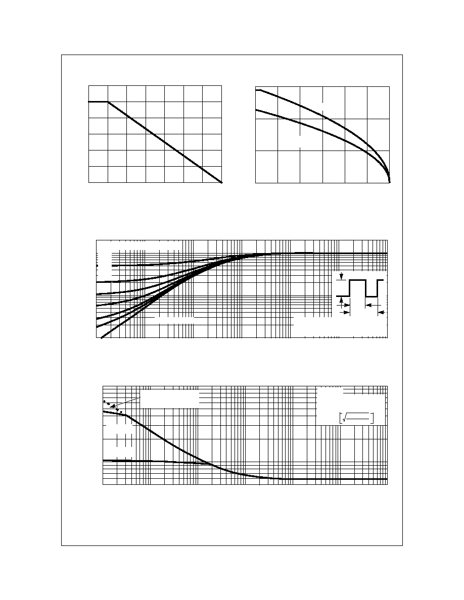
Typical Characteristic
Figure 1. Normalized Power Dissipation vs
Ambient Temperature
Figure 2. Maximum Continuous Drain Current vs
Case Temperature
Figure 3. Normalized Maximum Transient Thermal Impedance
Figure 4. Peak Current Capability
T
C
, CASE TEMPERATURE (
o
C)
PO
WER DISSIP
A
TION MUL
TIPLIER
0
0
25
50
75
100
175
0.2
0.4
0.6
0.8
1.0
1.2
125
150
0
20
40
60
25
50
75
100
125
150
175
I
D
,
DRAIN CURRENT (A)
T
C
, CASE TEMPERATURE (
o
C)
V
GS
= 4.5V
V
GS
= 10V
0.1
1
10
-5
10
-4
10
-3
10
-2
10
-1
10
0
10
1
0.01
2
t, RECTANGULAR PULSE DURATION (s)
Z
JC
,
NORMALIZED
THERMAL IMPED
ANCE
NOTES:
DUTY FACTOR: D = t
1
/t
2
PEAK T
J
= P
DM
x Z
JC
x R
JC
+ T
C
P
DM
t
1
t
2
0.5
0.2
0.1
0.05
0.01
0.02
DUTY CYCLE - DESCENDING ORDER
SINGLE PULSE
100
1000
10
-5
10
-4
10
-3
10
-2
10
-1
10
0
10
1
50
I
DM
,
PEAK CURRENT (A)
t, PULSE WIDTH (s)
TRANSCONDUCTANCE
MAY LIMIT CURRENT
IN THIS REGION
T
C
= 25
o
C
I = I
25
175 - T
C
150
FOR TEMPERATURES
ABOVE 25
o
C DERATE PEAK
CURRENT AS FOLLOWS:
V
GS
= 10V
V
GS
= 5V
©2002 Fairchild Semiconductor Corporation
Rev. B, January 2002
ISL9N312AP3/ISL9N312AS3ST
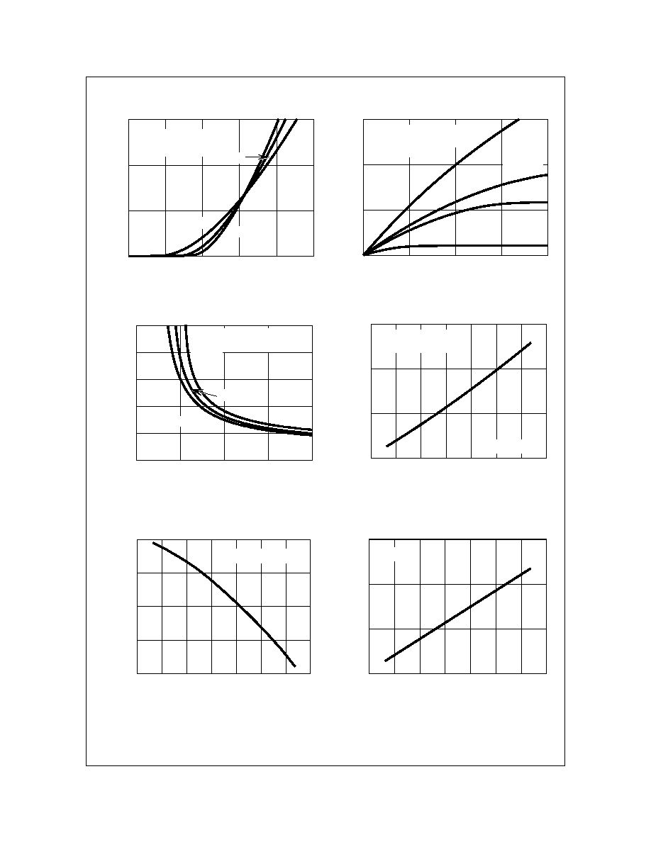
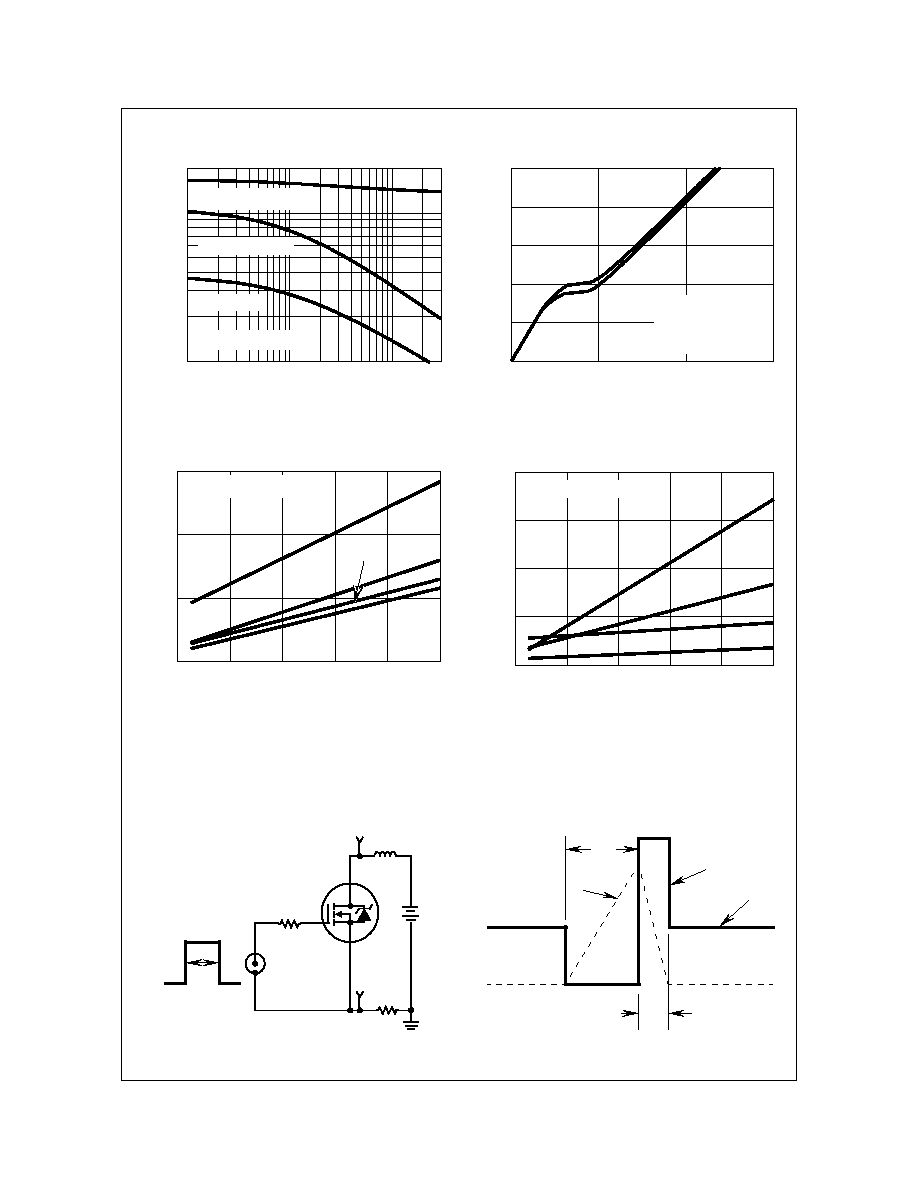
Figure 5. Transfer Characteristics
Figure 6. Saturation Characteristics
Figure 7. Drain to Source On Resistance vs Gate
Voltage and Drain Current
Figure 8. Normalized Drain to Source On
Resistance vs Junction Temperature
Figure 9. Normalized Gate Threshold Voltage vs
Junction Temperature
Figure 10. Normalized Drain to Source
Breakdown Voltage vs Junction Temperature
Typical Characteristic
(Continued)
0
40
80
120
1
2
3
4
5
6
I
D
,
DRAIN CURRENT (A)
V
GS
, GATE TO SOURCE VOLTAGE (V)
PULSE DURATION = 80ms
DUTY CYCLE = 0.5% MAX
V
DD
= 15V
T
J
= -55
o
C
T
J
= 175
o
C
T
J
= 25
o
C
0
40
80
120
0
0.5
1.0
1.5
2.0
I
D
,
DRAIN CURRENT (A)
V
DS
, DRAIN TO SOURCE VOLTAGE (V)
PULSE DURATION = 80
µ
µ
µ
µs
DUTY CYCLE = 0.5% MAX
V
GS
= 3V
T
C
= 25
o
C
V
GS
= 10V
V
GS
= 4.5V
V
GS
= 4V
5
10
15
20
25
2
4
6
8
10
30
I
D
= 12A
V
GS
, GATE TO SOURCE VOLTAGE (V)
I
D
= 58A
r
DS(ON)
,
DRAIN
T
O
SOURCE
ON RESIST
ANCE (m
)
PULSE DURATION = 80
µ
µ
µ
µs
DUTY CYCLE = 0.5% MAX
I
D
= 32A
0.5
1.0
1.5
2.0
-80
-40
0
40
80
120
160
200
NORMALIZED DRAIN
T
O
SOURCE
T
J
, JUNCTION TEMPERATURE (
o
C)
ON RESIST
ANCE
V
GS
= 10V, I
D
= 58A
PULSE DURATION = 80
µ
µ
µ
µs
DUTY CYCLE = 0.5% MAX
0.4
0.6
0.8
1.0
1.2
-80
-40
0
40
80
120
160
200
NORMALIZED GA
TE
T
J
, JUNCTION TEMPERATURE (
o
C)
V
GS
= V
DS
, I
D
= 250
µ
µ
µ
µA
THRESHOLD V
O
L
T
A
G
E
0.9
1.0
1.1
1.2
-80
-40
0
40
80
120
160
200
T
J
, JUNCTION TEMPERATURE (
o
C)
NORMALIZED DRAIN
T
O
SOURCE
I
D
= 250
µ
µ
µ
µA
BREAKDO
WN V
O
L
T
A
G
E
©2002 Fairchild Semiconductor Corporation
Rev. B, January 2002
ISL9N312AP3/ISL9N312AS3ST
Figure 11. Capacitance vs Drain to Source
Voltage
Figure 12. Gate Charge Waveforms for Constant
Gate Currents
Figure 13. Switching Time vs Gate Resistance
Figure 14. Switching Time vs Gate Resistance
Typical Characteristic
(Continued)
100
1000
0.1
1
10
30
2000
C,
CAP
A
CIT
ANCE (pF)
V
DS
, DRAIN TO SOURCE VOLTAGE (V)
V
GS
= 0V, f = 1MHz
C
ISS
= C
GS
+ C
GD
C
OSS
C
GS
+ C
GD
C
RSS
= C
GD
0
2
4
6
8
10
0
10
20
30
V
GS
,
GA
TE
T
O
SOURCE
V
O
L
T
A
GE (V)
Q
g
, GATE CHARGE (nC)
V
DD
= 15V
I
D
= 58A
I
D
= 32A
WAVEFORMS IN
DESCENDING ORDER:
0
50
100
150
0
10
20
30
40
50
SWITCHING TIME
(ns)
R
GS
, GATE TO SOURCE RESISTANCE (
)
V
GS
= 4.5V, V
DD
= 15V, I
D
= 12A
t
d(OFF)
t
r
t
f
t
d(ON)
0
50
100
150
200
0
10
20
30
40
50
SWITCHING TIME
(ns)
R
GS
, GATE TO SOURCE RESISTANCE (
)
V
GS
= 10V, V
DD
= 15V, I
D
= 12A
t
d(OFF)
t
r
t
d(ON)
t
f
Test Circuits and Waveforms
Figure 15. Unclamped Energy Test Circuit
Figure 16. Unclamped Energy Waveforms
t
P
V
GS
0.01
L
I
AS
+
-
V
DS
V
DD
R
G
DUT
VARY t
P
TO OBTAIN
REQUIRED PEAK I
AS
0V
V
DD
V
DS
BV
DSS
t
P
I
AS
t
AV
0