
©2006 Fairchild Semiconductor Corporation
1
www.fairchildsemi.com
FKN08PN40 Rev. A
FKN08PN40 TRIAC (Silicon
Bidirectional Thyristor)
tm
August 2006
FKN08PN40
TRIAC (Silicon Bidirectional Thyristor)
Application Explanation
∑ Switching mode power supply, light dimmer, electric flasher unit, hair drier
∑ TV sets, stereo, refrigerator, washing machine
∑ Electric blanket, solenoid driver, small motor control
∑ Photo copier, electric tool
Absolute Maximum Ratings
T
a
= 25∞C unless otherwise noted
Thermal Characteristics
Note1: Infinite cooling condition.
Note2: JESD51-10 ( Test Borad: FR4 3.0"*4.5"*0.062", Minimum land pad)
Symbol
Parameter
Value
Rating
Units
V
DRM
V
RRM
Peak Repetitive Off-State Voltage
Sine Wave 50 to 60Hz, Gate Open
400
V
I
T (RMS)
RMS On-State Current
Commercial frequency, sine full wave
360
∞
conduction, Tc= 70
0.8
A
I
TSM
Surge On-State Current
Sinewave 1 full cycle, peak value,
non-repetitive
50Hz
8
A
60Hz
9
A
I
2
t
I
2
t for Fusing
Value corresponding to 1 cycle of halfwave,
surge on-state current, tp=8.4ms
0.33
A
2
s
P
GM
Peak Gate Power Dissipation
5
W
P
G (AV)
Average Gate Power Dissipation
0.1
W
V
GM
Peak Gate Voltage
5
V
I
GM
Peak Gate Current
1
A
T
J
Junction Temperature
- 40 ~ 125
∞
C
T
STG
Storage Temperature
- 40 ~ 125
∞
C
Symbol
Parameter
Value
Units
R
JC
Thermal Resistance, Junction to Case
(note1)
40
∞
C/W
R
JA
Thermal Resistance, Junction to Ambient
(note2)
160
∞
C/W
1
3
2
1: T
1
2: Gate
3: T
2
1 2 3
TO-92

2
www.fairchildsemi.com
FKN08PN40 Rev. A
FKN08PN40 TRIAC (Silicon
Bidirectional Thyristor)
Electrical Characteristics
T
C
= 25∞C unless otherwise noted
Commutation dv/dt Test
Symbol
Parameter
Test Condition
Min.
Typ.
Max.
Units
I
DRM
I
RRM
Repetieive Peak Off-State Current
V
DRM
/V
RRM
applied
-
-
100
µ
A
V
TM
On-State Voltage
T
C
=25
∞
C, I
TM
=1.12A
Instantaneous measurement
-
-
1.8
V
V
GT
Gate Trigger Voltage
I
V
D
=12V, R
L
=100
T2(+), Gate (+)
-
-
2.0
V
II
T2(+), Gate (-)
-
-
2.0
V
III
T2(-), Gate (-)
-
-
2.0
V
I
GT
Gate Trigger Current
I
V
D
=12V, R
L
=100
T2(+), Gate (+)
-
-
5
mA
II
T2(+), Gate (-)
-
-
5
mA
III
T2(-), Gate (-)
-
-
5
mA
V
GD
Gate Non-Trigger Voltage
T
J
=125
∞
C, V
D
=1/2V
DRM
0.2
-
-
V
I
H
Holding Current (I, II,III)
V
D
= 12V, I
TM
= 200mA
-
-
15
mA
I
L
Latching Current
I, III
V
D
= 12V, I
G
= 10mA
-
-
15
mA
II
-
-
20
mA
dv/dt(s)
Critical Rate of Rise of
Off-State Voltag
V
DRM
= 63% Rated, T
j
= 125
∞
C,
Exponential Rise
20
-
-
V/
µ
s
dv/dt(c)
Critical-Rate of Rise of Off-State Com-
mutating Voltage (di/dt=-0.7A/mS)
3.0
-
-
V/
µ
s
V
DRM
(V)
Test Condition
Commutating voltage and current waveforms
(inductive load)
FKN08PN40
1. Junction Temperature
T
J
=125
∞
C
2. Rate of decay of on-state
commutating current (di/dt)
C
3. Peak off-state voltage
V
D
= 200V
Supply Voltage
Main Current
Main Voltage
Time
Time
Time
V
D
(dv/dt)
C
(di/dt)
C

4
www.fairchildsemi.com
FKN08PN40 Rev. A
FKN08PN40 TRIAC (Silicon
Bidirectional Thyristor)
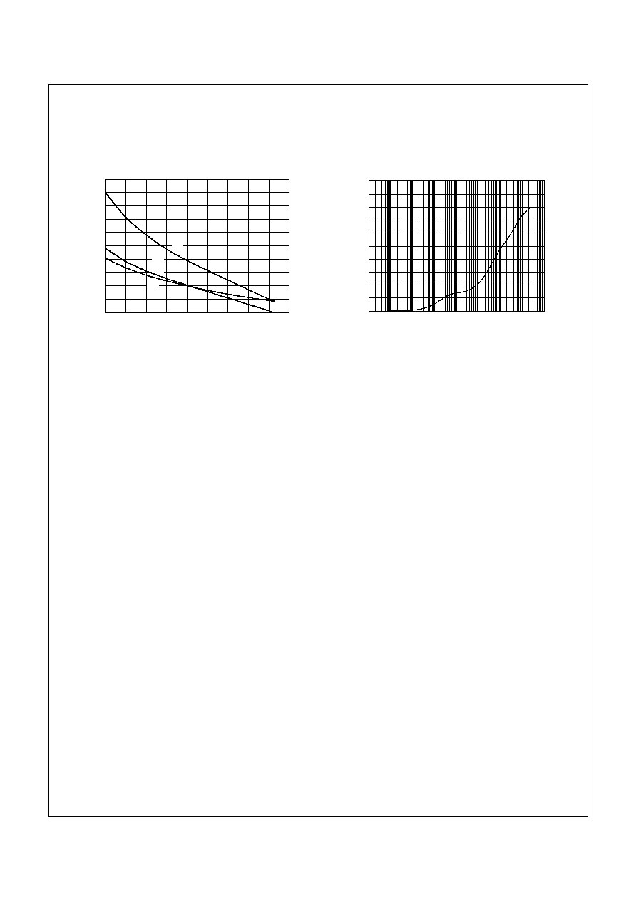
Typical Performance Characteristics
Figure 1. On-State Characteristics
Figure 2. Power Dissipation
Figure 3. RMS Current Rating
Figure 4. Typical Gate Trigger Current
vs Junction Temperature
Figure5. Typical Gate Voltage
vs Junction Temperarure
Figure6. Typical Latching Currrent
vs Junction Temperature
0.1
1
0.0
0.5
1.0
1.5
2.0
2.5
T
J
=125
o
C
T
J
=25
o
C
V
TM
[V], On-State Voltage
I
TM
[
A
], O
n
-S
ta
t
e
C
u
rr
e
n
t
0.0
0.2
0.4
0.6
0.8
1.0
0.0
0.2
0.4
0.6
0.8
1.0
1.2
DC
180
o
120
o
90
o
60
o
30
o
P
AV
[
W
]
,
M
axim
u
m Av
er
ag
e Po
w
e
r
Dis
s
ip
at
i
o
n
IT
RMS
[A], On-State Current
0.0
0.1
0.2
0.3
0.4
0.5
0.6
0.7
0.8
0.9
1.0
70
80
90
100
110
120
DC
180
o
120
o
90
o
60
o
30
o
Max
i
mum Al
lowa
ble Ca
se
T
e
mperature,
T
C
[
o
C]
IT
RMS
[A], On-State Current
-40
0
40
80
120
0
1
2
3
4
5
6
Q3
Q1
I
GT
[m
A],
G
a
te
T
r
i
g
g
e
r
C
u
r
r
e
n
t
T
J
[
o
C], Junction Temperature
Q2
-40
0
40
80
120
0.4
0.5
0.6
0.7
0.8
0.9
1.0
Q3
Q1
V
GT
[m
A], Ga
te T
r
i
g
g
e
r
Vo
lta
g
e
T
J
[
o
C], Junction Temperature
Q2
-40
0
40
80
120
0
2
4
6
Q3
Q1
V
GT
[mA
], G
a
te T
r
i
gge
r V
o
l
t
age
T
J
[
o
C], Junction Temperature
5
www.fairchildsemi.com
FKN08PN40 Rev. A
FKN08PN40 TRIAC (Silicon
Bidirectional Thyristor)
Typical Performance Characteristics
(Continued)
Figure7. Typical Holding Current
vs Junction Temperature
Figure8. Junction to Case Thermal Resistance
-40
0
40
80
120
0
1
2
3
4
5
Q3
Q2
Q1
I
H
[m
A],Ho
l
d
i
ng
Cu
rre
n
t
T
J
[
o
C], Junction Temperature
1E-6
1E-5
1E-4
1E-3
0.01
0.1
1
10
100
0
10
20
30
40
50
Junct
i
on
to C
a
se T
herm
a
l
Resistance,
[
o
C/
W]
Time, [S]
