©2000 Fairchild Semiconductor International
www.fairchildsemi.com
Rev. .5.0
Features
∑ Precision fixed operating frequency
∑
KA1L0380B/KA1L0380RB
(50KHz)
∑
KA1M0380RB
(67KHz)
∑
KA1H0380RB
(100KHz)
∑ Pulse by pulse over current limiting
∑ Over load protection
∑ Over voltage protection (Min. 23V)
∑ Internal thermal shutdown function
∑ Under voltage lockout
∑ Internal high voltage sense FET
∑ Auto restart (
KA1L0380RB/KA1M0380RB/KA1H0380RB)
Description
The SPS product family is specially designed for an off-line
SMPS with minimal external components. The SPS consist of
high voltage power SenseFET and current mode PWM control-
ler IC. PWM controller features integrated fixed oscillator,
under voltage lock out, leading edge blanking, optimized gate
turn-on/turn-off driver, thermal shut down protection, over volt-
age protection, temperature compensated precision current
sources for loop compensation and fault protection circuit.
Compared to discrete MOSFET and controller or RCC switch-
ing converter solution, a SPS can reduce total component count,
design size, weight and at the same time increase & efficiency,
productivity, and system reliability. It has a basic platform well
suited for cost effective design in either a flyback converter or a
forward converter.
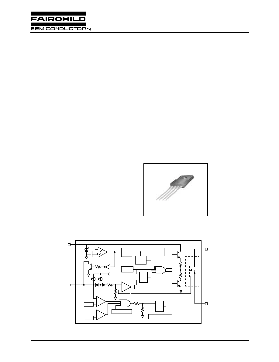
TO-220F-4L
1. GND 2. DRAIN 3. V
CC
4. FB
1
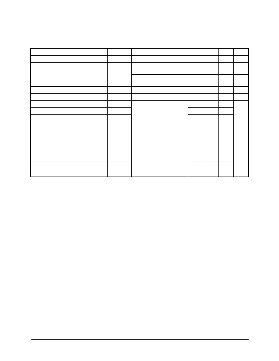
Internal Block Diagram
#3 V
CC
32V
5
µ
A
9V
2.5R
1R
1mA
0.1V
+
-
OVER VOLTAGE S/D
+
-
7.5V
25V
Thermal S/D
S
R
Q
Power on reset
+
-
L.E.B
S
R
Q
OSC
5V
Vref
Internal
bias
Good
logic
SFET
#2 DRAIN
#1 GND
#4 FB
KA1L0380B/KA1L0380RB/KA1M0380RB/
KA1H0380RB
Fairchild Power Switch(SPS)

KA1L0380B/KA1L0380RB/KA1M0380RB/KA1H0380RB
2
Absolute Maximum Ratings
Notes:
1. Tj=25
∞
C to 150
∞
C
2. Repetitive rating: Pulse width limited by maximum junction temperature
3. L=51mH, V
DD
=50V, R
G
=25
, starting Tj=25
∞
C
4. L=13
µ
H, starting Tj=25
∞
C
Parameter
Symbol
Value
Unit
Drain-source (GND) voltage
(1)
V
DSS
800
V
Drain-Gate voltage (R
GS
=1M
)
V
DGR
800
V
Gate-source (GND) voltage
V
GS
±
30
V
Drain current pulsed
(2)
I
DM
12
A
DC
Single pulsed avalanche energy
(3)
E
AS
95
mJ
Avalanche current
(4)
I
AS
6
A
Continuous drain current (T
C
=25
∞
C)
I
D
3.0
A
DC
Continuous drain current (T
C
=100
∞
C)
I
D
2.1
A
DC
Supply voltage
V
CC
30
V
Analog input voltage range
V
FB
-
0.3 to V
SD
V
Total power dissipation
P
D
35
W
Derating
0.28
W/
∞
C
Operating temperature
T
OPR
-
25 to +85
∞
C
Storage temperature
T
STG
-
55 to +150
∞
C
KA1L0380B/KA1L0380RB/KA1M0380RB/KA1H0380RB
3
Electrical Characteristics (SFET part)
(Ta=25
∞
C unless otherwise specified)
Note:
Pulse test: Pulse width
300
µ
S, duty cycle
2%
Parameter
Symbol
Condition
Min.
Typ.
Max.
Unit
Drain-source breakdown voltage
BV
DSS
V
GS
=0V, I
D
=50
µ
A
800
-
-
V
Zero gate voltage drain current
I
DSS
V
DS
=Max., Rating,
V
GS
=0V
-
-
50
µ
A
V
DS
=0.8Max., Rating,
V
GS
=0V, T
C
=125
∞
C
-
-
200
µ
A
Static drain-source on resistance
(Note)
R
DS(ON)
V
GS
=10V, I
D
=1.5A
-
4.0
5.0
Forward transconductance
(Note)
gfs
V
DS
=15V, I
D
=1.5A
1.5
2.5
-
S
Input capacitance
Ciss
V
GS
=0V, V
DS
=25V,
f=1MHz
-
779
-
pF
Output capacitance
Coss
-
75.6
-
Reverse transfer capacitance
Crss
-
24.9
-
Turn on delay time
td(on)
V
DD
=0.5BV
DSS
, I
D
=3.0A
(MOSFET switching
time are essentially
independent of
operating temperature)
-
40
-
nS
Rise time
tr
-
95
-
Turn off delay time
td(off)
-
150
-
Fall time
tf
-
60
-
Total gate charge
(gate-source+gate-drain)
Qg
V
GS
=10V, I
D
=3.0A,
V
DS
=0.5BV
DSS
(MOSFET
switching time are
essentially independent of
operating temperature)
-
-
34
nC
Gate-source charge
Qgs
-
7.2
-
Gate-drain (Miller) charge
Qgd
-
12.1
-
S
1
R
----
=
KA1L0380B/KA1L0380RB/KA1M0380RB/KA1H0380RB
4
Electrical Characteristics (CONTROL part)
(Ta=25
∞
C unless otherwise specified)
Notes:
1. These parameters, although guaranteed, are not 100% tested in production
2. These parameters, although guaranteed, are tested in EDS (wafer test) process
Parameter
Symbol
Condition
Min.
Typ.
Max.
Unit
REFERENCE SECTION
Output voltage
(1)
Vref
Ta=25
∞
C
4.80
5.00
5.20
V
Temperature Stability
(1)(2)
Vref/
T
-
25
∞
C
Ta
+85
∞
C
-
0.3
0.6
mV/
∞
C
OSCILLATOR SECTION
Initial accuracy
F
OSC
KA1L0380B
45
50
55
kHz
KA1L0380RB
45
50
55
KA1M0380RB
61
67
73
KA1H0380RB
90
100
110
Frequency change with temperature
(2)
F/
T
-
25
∞
C
Ta
+85
∞
C
-
±
5
±
10
%
PWM SECTION
Maximum duty cycle
Dmax
KA1L0380B
74
77
80
%
KA1L0380RB
74
77
80
KA1M0380RB
74
77
80
KA1H0380RB
64
67
70
FEEDBACK SECTION
Feedback source current
I
FB
Ta=25
∞
C, 0V
Vfb
3V
0.7
0.9
1.1
mA
Shutdown delay current
Idelay
Ta=25
∞
C, 5V
Vfb
V
SD
4.0
5.0
6.0
µ
A
OVER CURRENT PROTECTION SECTION
Over current protection
I
L(max)
Max. inductor current
1.89
2.15
2.41
A
UVLO SECTION
Start threshold voltage
Vth(H)
-
14
15
16
V
Minimum operating voltage
Vth(L)
After turn on
9
10
11
V
TOTAL STANDBY CURRENT SECTION
Start current
I
ST
V
CC
=14V
0.1
0.3
0.45
mA
Operating supply current
(control part only)
I
OPR
Ta=25
∞
C
6
12
18
mA
V
CC
zener voltage
V
Z
I
CC
=20mA
30
32.5
35
V
SHUTDOWN SECTION
Shutdown Feedback voltage
V
SD
-
6.9
7.5
8.1
V
Thermal shutdown temperature (Tj)
(1)
T
SD
-
140
160
-
∞
C
Over voltage protection voltage
V
OVP
-
23
25
28
V
KA1L0380B/KA1L0380RB/KA1M0380RB/KA1H0380RB
5
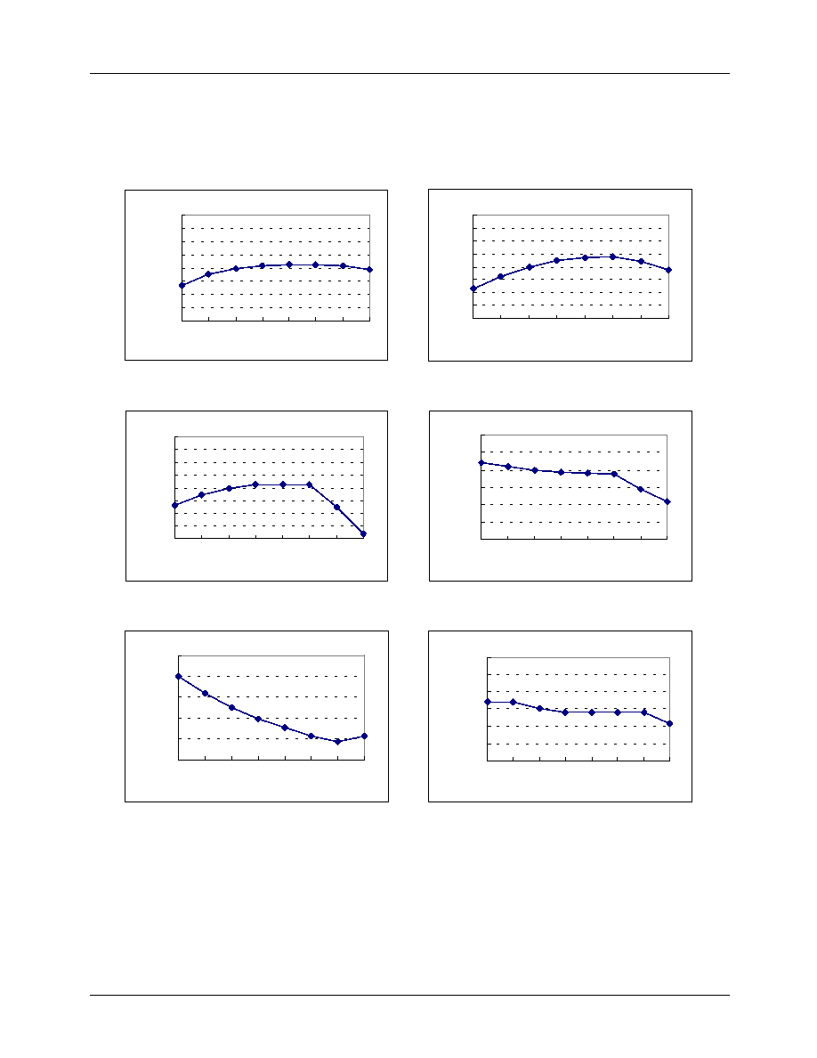
Typical Performance Characteristics
(These characteristic graphs are normalized at Ta=25
∞
C)
Fig.1 Operating Frequency
0.8
0.85
0.9
0.95
1
1.05
1.1
1.15
1.2
-25
0
25
50
75
100 125 150
Fosc
Fig.2 Feedback Source Current
0.8
0.85
0.9
0.95
1
1.05
1.1
1.15
1.2
-25
0
25
50
75
100 125 150
Ifb
Fig.3 Operating Current
0.8
0.85
0.9
0.95
1
1.05
1.1
1.15
1.2
-25
0
25
50
75
100 125 150
Iop
Fig.4 Max Inductor Current
0.8
0.85
0.9
0.95
1
1.05
1.1
-25
0
25
50
75
100 125 150
Ipeak
Fig.5 Start up Current
0.5
0.7
0.9
1.1
1.3
1.5
-25
0
25
50
75
100 125 150
Istart
Fig.6 Start Threshold Voltage
0.85
0.9
0.95
1
1.05
1.1
1.15
-25
0
25
50
75 100 125 150
Vstart
Temperature [
∞
C
]
Temperature [
∞
C
]
Temperature [
∞
C
]
Temperature [
∞
C
]
Temperature [
∞
C
]
Temperature [
∞
C
]
Figure 1. Operating Frequency
Figure 2. Feedback Source Current
Figure 3. Operating Current
Figure 4. Max. Inductor Current
Figure 5. Start up Current
Figure 6. Start Threshold Voltage
I
L(MAX)
I
ST
V
th(H)
I
OPR