 | –≠–ª–µ–∫—Ç—Ä–æ–Ω–Ω—ã–π –∫–æ–º–ø–æ–Ω–µ–Ω—Ç: KA278R05 | –°–∫–∞—á–∞—Ç—å:  PDF PDF  ZIP ZIP |
©2002 Fairchild Semiconductor Corporation
www.fairchildsemi.com
Rev. 1.0.2
Features
∑ 2A/5V Output Low Dropout Voltage Regulator
∑ TO-220 Full-Mold Package (4Pin)
∑ Overcurrent Protection, Thermal Shutdown
∑ Overvoltage Protection, Short Circuit Protection
∑ With Output Disable Function
Description
The KA278R05 is a low-dropout voltage regulator suitable
for various electronic equipments. It provides constant
voltage power source with TO-220 4 lead full mold package.
The dropout voltage of KA278R05 is below 0.5V in full
rated current(2A). This regulator has various functions such
as a peak current protection, a thermal shut down, an
overvoltage protection and an output disable function.
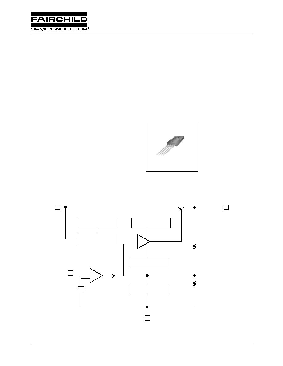
TO-220F-4L
1.Vin 2. Vo 3. GND 4. Vdis
1
Internal Block Diagram
THERMAL SHUTDOWN
BANDGAP REFERENCE
OVERVOLTAGE
PROTECTION
SOA PROTECTION
SHORTCIRCUIT
PROTECTION
1
4
3
2
Vin
Vdis
Vo
GND
HIGH / LOW
OUTPUT
ON / OFF
Q1
R1
R2
-
+
-
+
1.4V
SHORT-CIRCUIT
KA278R05
Low Dropout Voltage Regulator
KA278R05
2
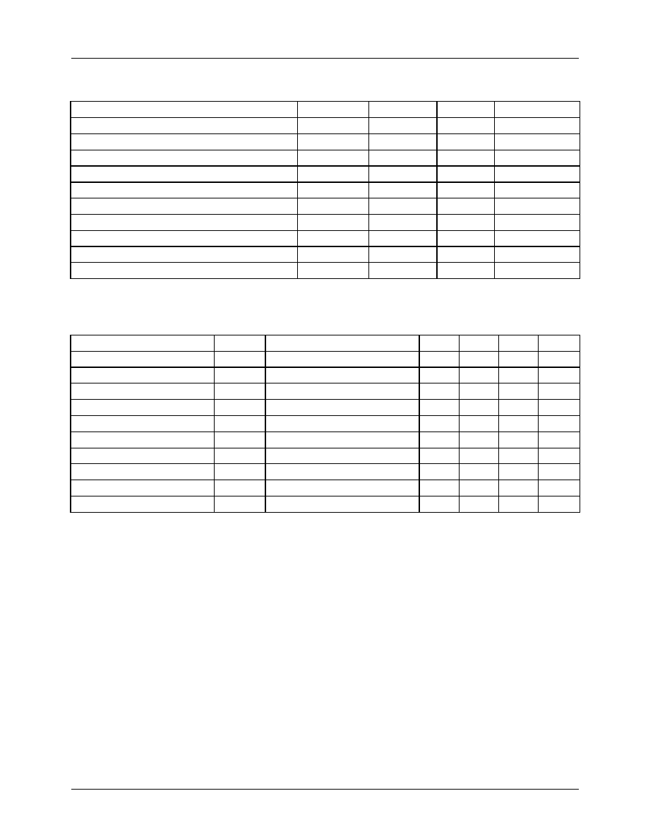
Absolute Maximum Ratings
Electrical Characteristics
(Vin=7V, Io=1.0A, Ta=25
∞
C , unless otherwise specified)
Note:
1.These parameters, although guaranteed, are not 100% tested in production.
2. Junction -to -case thermal resistance test environments.
-. Pneumatic heat sink fixture.
-. Clamping pressure 60psi through 12mm diameter cylinder.
-. Thermal grease applied between PKG and heat sink fixture
Parameter
Symbol
Value
Unit
Remark
Input Voltage
Vin
35
V
-
Disable Voltage
Vdis
35
V
-
Output Current
Io
2.0
A
-
Power Dissipation 1
Pd1
1.5
W
No Heatsink
Power Dissipation 2
Pd2
15
W
With Heatsink
Junction Temperature
Tj
150
∞
C
-
Operating Temperature
Topr
-20 ~ 80
∞
C
-
Thermal Resistance, Junction-to Case (Note2)
R
jc
2.9
∞
C/W
-
Thermal Resistance, Junction-to-Air (Note2)
R
ja
48.51
∞
C/W
-
Thermal Shutdown Temperature
Ttsd
150
∞
C
-
Parameter
Symbol
Conditions
Min.
Typ.
Max.
Unit
Output Voltage
Vo
-
4.88
5
5.12
V
Load Regulation
Rload
5mA < Io < 2A
-
0.1
2.0
%
Line Regulation
Rline
6V < Vin < 12V
-
0.5
2.5
%
Ripple Rejection Ratio
RR
note1
45
55
-
dB
Dropout Voltage
Vdrop
Io = 2A
-
-
0.5
V
Disable Voltage High
VdisH
Output Active
2.0
-
-
V
Disable Voltage Low
VdisL
Output Disabled
-
-
0.8
V
Disable Bias Current High
IdisH
Vdis = 2.7V
-
-
20
µ
A
Disable Bias Current Low
IdisL
Vdis = 0.4V
-
-
-0.4
mA
Quiescent Current
Iq
Io = 0A
-
-
10
mA

KA278R05
3
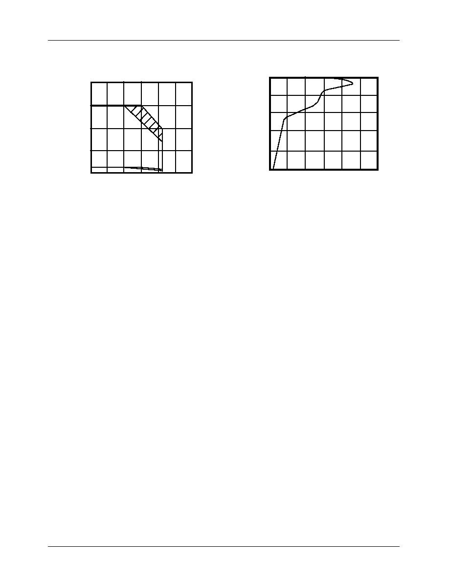
Typical Performance Characteristics
Figure 1. Output Voltage vs. Input Voltage
Figure 3. Output Voltage vs. Disable Voltage
Figure 5. Quiescent Current vs. Temperature(Tj)
Figure 2. Quiescent Current vs. Input Voltage
Figure 4. Output Voltage vs. Temperature(Tj)
Figure 6. Dropout Voltage vs. Junction Temperature
5
10
15
Input voltage Vin (V)
6
5
4
3
2
1
7
0
0
O
u
tp
u
t
v
o
l
t
a
g
e
V
o
(
V
)
RL=
RL=2.5
8
7
6
5
4
3
0
0
O
u
tput vol
t
ag
e
V
o
(V
)
3
Disable voltage Vdis (V)
0.5
1.5
2
1
1
2
2.5
8
6
4
2
0
Q
u
i
e
scent
cur
r
e
n
t
I
q
(
m
A
)
Junction temperature Tj(
o
C)
75
125
0
25
50
100
-25
50
40
30
20
10
0
0
Qu
i
e
s
c
e
n
t cu
rre
nt
Iq
(m
A
)
15
Input voltage Vin (V)
5
10
RL=
5.04
5.02
5.00
5.06
-25
O
u
t
put
v
o
l
t
ag
e
V
o
(
V
)
TEMPERATURE Tj(
o
C)
75
125
0
25
50
100
4.96
4.94
4.92
4.98
Temperature Tj(
∞
C)
125
0.6
0.5
0.4
0.3
0
D
r
op
out
volt
ag
e
V
d
r
o
p
(
V
)
Junction temperature Tj(
o
C)
0.2
0.1
75
0
25
50
100
-25
Io=2A
1.5A
1.0A
0.5A
KA278R05
4
Typical Performance Characteristics
(Continued)
Figure 7. Power Dissipation vs. Temperature(Ta)
Figure 8. Overcurrent Protection Characteristics
(Typical Value)
-25
P
o
w
e
r
dis
s
ip
ation
P
D
(W
)
TEMPERATURE Tj(
o
C)
75
125
0
25
50
100
15
10
5
20
0
TEMPERATURE Ta
(
∞
C)
D
Temperature Ta(
∞
C)
Output Current(A)
R
e
l
a
t
i
v
e
o
u
t
p
ut
v
o
l
t
ag
e(
%
)
3.0
5.0
0
1.0
2.0
4.0
80
60
20
0
40
6.0
Output Current(A)
R
e
l
a
t
i
v
e
o
u
t
p
ut
v
o
l
t
ag
e(
%
)
3.0
5.0
0
1.0
2.0
4.0
80
60
20
0
40
6.0

KA278R05
5
Typical Application
Figure 1. Application Circuit
∑ Ci is required if regulator is located an appreciable distance from power supply filter.
∑ Co improves stability and transient response.(Co > 47
µ
F)
+
+
1
2
3
4
Vin
Vdis
Vo
GND
Disable Signal
KA278R05
6
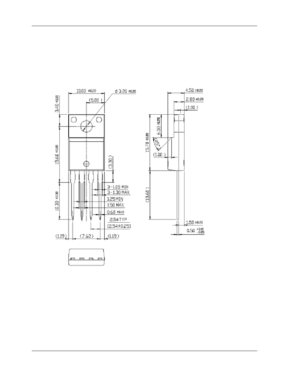
Mechanical Dimensions
Package
Dimensions in millimeters
TO-220F-4L

KA278R05
7
Mechanical Dimensions
(Continued)
Package
Dimensions in millimeters
TO-220F-4L(Forming)

KA278R05
9/10/02 0.0m 001
Stock#DSxxxxxxxx
2002 Fairchild Semiconductor Corporation
LIFE SUPPORT POLICY
FAIRCHILD'S PRODUCTS ARE NOT AUTHORIZED FOR USE AS CRITICAL COMPONENTS IN LIFE SUPPORT DEVICES
OR SYSTEMS WITHOUT THE EXPRESS WRITTEN APPROVAL OF THE PRESIDENT OF FAIRCHILD SEMICONDUCTOR
CORPORATION. As used herein:
1. Life support devices or systems are devices or systems
which, (a) are intended for surgical implant into the body,
or (b) support or sustain life, and (c) whose failure to
perform when properly used in accordance with
instructions for use provided in the labeling, can be
reasonably expected to result in a significant injury of the
user.
2. A critical component in any component of a life support
device or system whose failure to perform can be
reasonably expected to cause the failure of the life support
device or system, or to affect its safety or effectiveness.
www.fairchildsemi.com
DISCLAIMER
FAIRCHILD SEMICONDUCTOR RESERVES THE RIGHT TO MAKE CHANGES WITHOUT FURTHER NOTICE TO ANY
PRODUCTS HEREIN TO IMPROVE RELIABILITY, FUNCTION OR DESIGN. FAIRCHILD DOES NOT ASSUME ANY
LIABILITY ARISING OUT OF THE APPLICATION OR USE OF ANY PRODUCT OR CIRCUIT DESCRIBED HEREIN; NEITHER
DOES IT CONVEY ANY LICENSE UNDER ITS PATENT RIGHTS, NOR THE RIGHTS OF OTHERS.
Ordering Information
Product Number
Package
Operating Temperature
KA278R05TU TO-220F-4L
-20
∞
C to +80
∞
C
KA278R05YDTU
TO-220F-4L(Forming)