©2000 Fairchild Semiconductor International
www.fairchildsemi.com
Rev. 1.0.2
May. 2000.
1
Features
∑ Built-in power save circuit
∑ Built-in current limit circuit
∑ Built-in thermal shutdown circuit (TSD)
∑ Built-in hall bias
∑ Built-in FG signal output circuit
∑ Built-in rotational direction detecting circuit
∑ Built-in protection circuit for reverse rotation
∑ Built-in short brake circuit
∑ Built-in variable-regulator
∑ Built-in 4-CH balanced transformerless (BTL) driver
∑ Built-in BTL mute circuit (CH1/2, CH3 and CH4)
∑ Corresponds to 3.3V DSP
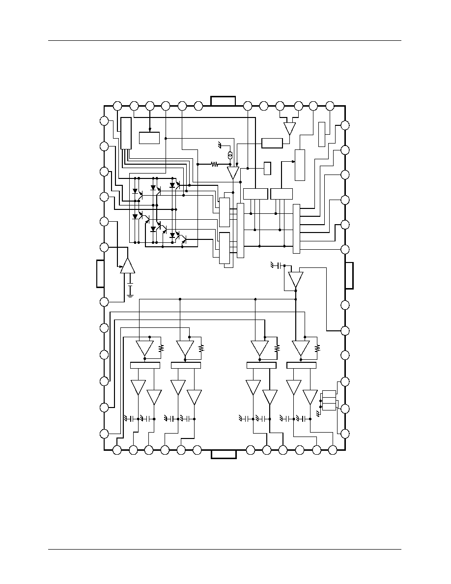
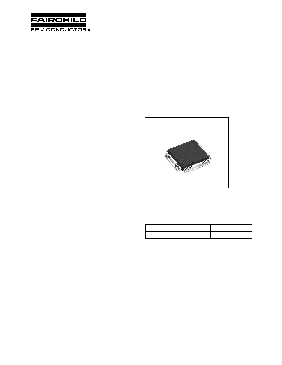
Description
The KA3014 is a monolithic integrated circuit suitable for a
4-ch motor driver which drives the tracking actuator, focus
actuator, sled motor, loading motor and 3-phase BLDC spin-
dle motor of the MDP/CAR-MD/CAR-NAVIGATION sys-
tem.
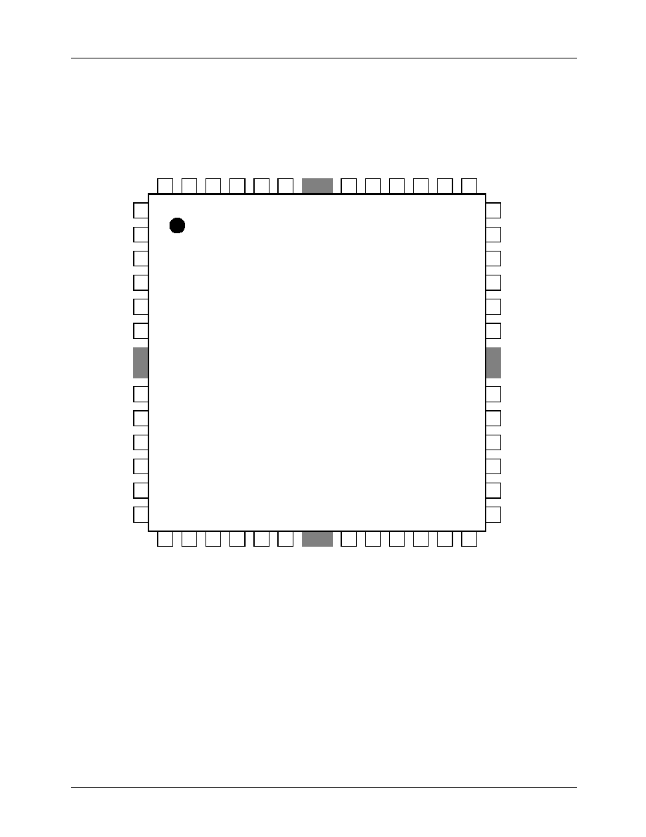
48-QFPH-1414
KA3014
Spindle + 4-CH Motor Driver
Target Application
∑ Mini disk player
∑ Digital video disk player
∑ Car mini disk player
∑ Car navigation system
Ordering Information
Device
Package
Operating Temp.
KA3014
48-QFPH-1414
-
35
∞
C ~ +85
∞
C

KA3014
3
Pin Definitions
Pin Number
Pin Name
I/O
Pin Function Descrition
1
VH
I
Hall bias
2
FG
O
FG signal output
3
ECR
I
Torque control reference
4
EC
I
Torque control signal
5
VCC2
-
Supply voltage
6
PC1
-
Phase compensation capacitor
7
SIGGND
-
Signal ground
8
VM
-
Motor supply voltage
9
CS1
I
Current sensor
10
S/S
I
Start/stop
11
DIR
O
3-phase rotational direction output
12
SB
I
Short brake
13
PWRGND
-
Power ground
14
A3
O
3-phase output 3
15
A2
O
3-phase output 2
16
A1
O
3-phase output 1
17
RESX
I
Variable regulator reset
18
VREGX
O
Variable regulator
19
REGOX
O
Variable regulator output
20
VCC1
-
Supply voltage
21
AVM12
-
BTL CH-1, 2 motor supply voltage
22
DI4
I
BTL drive input 4
23
DI3
I
BTL drive input 3
24
DI2
I
BTL drive input 2
25
DI1
I
BTL drive input 1
26
DO1
-
O
BTL drive 1 output (
-
)
27
DO1+
O
BTL drive 1 output (+)
28
DO2
-
O
BTL drive 2 output (
-
)
29
DO2+
O
BTL drive 2 output (+)
30
BTLPGND1
-
BTL power ground 1
31
BTLPGND2
≠
BTL power ground 2
KA3014
4
Pin Definitions (Continued)
Pin Number
Pin Name
I/O
Pin Function Descrition
32
DO3≠
O
BTL drive 3 output (≠)
33
DO3+
O
BTL drive 3 output (+)
34
AVM3
≠
BTL CH3 motor supply voltage
35
DO4≠
O
BTL drive 4 output (≠)
36
DO4+
O
BTL drive 4 output (+)
37
MUTE4
I
BTL drive mute CH 4
38
MUTE3
I
BTL drive mute CH 3
39
MUTE12
I
BTL drive mute CH 1, 2
40
AVM4
≠
BTL CH 4 motor supply voltage
41
BIAS
≠
BTL bias voltage
42
BTLSGND
≠
BTL drive signal ground
43
H1≠
I
Hall1(≠) input
44
H1+
I
Hall1(+) input
45
H2≠
I
Hall2(≠) input
46
H2+
I
Hall2(+) input
47
H3≠
I
Hall3(≠) input
48
H3+
I
Hall3(+) input