 | ÐлекÑÑоннÑй компоненÑ: KA3031 | СкаÑаÑÑ:  PDF PDF  ZIP ZIP |
Äîêóìåíòàöèÿ è îïèñàíèÿ www.docs.chipfind.ru
©2000 Fairchild Semiconductor International
www.fairchildsemi.com
Rev. 1.0.1
February. 2000.
1
Features
· 4-CH balanced transformerless (BTL) driver
· 2-CH (forward-reverse) control DC motor driver
· Operating supply voltage (4.5V ~ 16V)
· Built-in thermal shut down circuit (TSD)
· Built-in under voltage lockout circuit (UVLO)
· Built-in over voltage protection circuit (OVP)
· Built-in mute circuit (CH1, CH2, CH3 and CH4)
· Built-in normal op-amp
· Built-in 5V regulator with reset
Description
The KA3031 is a monolithic integrated circuit suitable for a
6-ch motor driver which drives the tracking actuator, focus
actuator, sled motor, tray motor, change motor and spindle
motor of the CDP/CAR-CD systems.
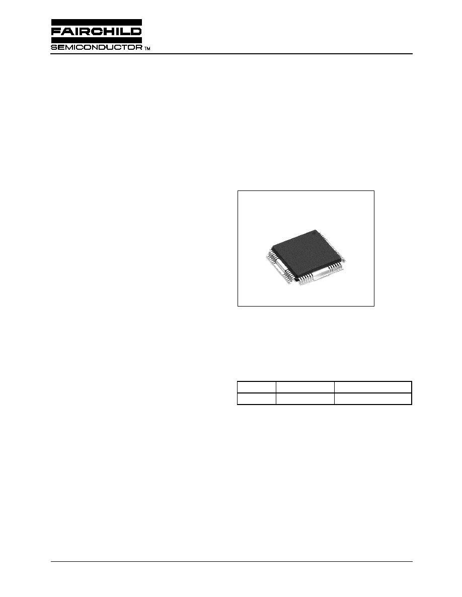
48-QFPH-1414
Typical Applications
· Compact disk player (CDP) with tray and changer
· Compact disk player (VCD) with tray and changer
· Automotive compact disk player (CDP) with tray and
changer
· Mixing with compact disk player (CDP) and mini disk
player (MD) with tray and changer
· Other compact disk media
Ordering Information
Device
Package
Operating Temp.
KA3031
48-QFPH-1414
-
35
°
C ~ +85
°
C
KA3031
6-Channel Motor Drive IC
KA3031
2
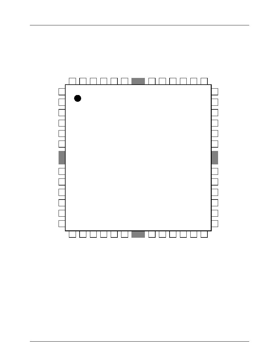
Pin Assignments
1
2
3
4
5
6
7
8
9
27
26
25
13
14
15
16
17
18
19
20
21
22
23
24
48
47
46
45
44
43
42
41
40
39
38
37
30
29
28
32
32
31
36
35
34
KA3031
IN1.2
OUT1
IN2.1
IN2.2
OUT2
IN3.1
IN3.2
OUT3
IN4.1
IN4.2
OUT4
CTL1
10
11
12
DO2.1
DO2.2
PGND3
DO3.1
DO3.2
PGND2
PGND1
DO4.1
DO4.2
DO5.1
DO5.2
DO6.1
FWD1 REV1
CTL FWD2 REV2 SGND
MUTE1MUTE2 MUTE3 MUTE4 PVCC1 DO6.2
IN1.1 REG50 REG050 REF SVCC RES50
OPIN(+)OPIN(
-
)OPOUT PVCC2 DO1.1 DO1.2
KA3031
3
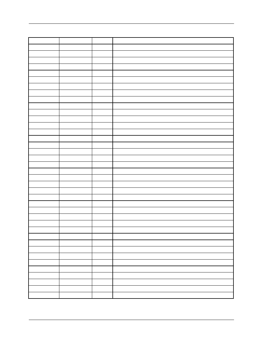
Pin Definitions
Pin Number
Pin Name
I/O
Pin Function Description
1
IN1.2
I
CH 1 op-amp input (
-
)
2
OUT1
O
CH 1 op-amp output
3
IN2.1
I
CH 2 op-amp input (+)
4
IN2.2
I
CH 2 op-amp input (
-
)
5
OUT2
O
CH 2 op-amp output
6
IN3.1
I
CH 3 op-amp input (+)
7
IN3.2
I
CH 3 op-amp input (
-
)
8
OUT3
O
CH 3 op-amp output
9
IN4.1
I
CH 4 op-amp input (+)
10
IN4.2
I
CH 4 op-amp input (
-
)
11
OUT4
O
CH 4 op-amp output
12
CTL1
I
CH 5 motor speed control
13
FWD1
I
CH 5 forward input
14
REW1
I
CH 5 reverse input
15
CTL2
I
CH 6 motor speed control
16
FWD2
I
CH 6 forward input
17
REW2
I
CH 6 reverse input
18
SGND
-
Signal ground
19
MUTE1
I
CH 1 mute
20
MUTE2
I
CH 2 mute
21
MUTE3
I
CH 3 mute
22
MUTE4
I
CH 4 mute
23
PVCC1
-
Power supply voltage (For CH 5, CH 6)
24
DO6.2
O
CH 6 drive output
25
DO6.1
O
CH 6 drive output
26
DO5.2
O
CH 5 drive output
27
DO5.1
O
CH 5 drive output
28
DO4.2
O
CH 4 drive output
29
DO4.1
O
CH 4 drive output
30
PGND
-
Power ground
31
PGND
-
Power ground
32
DO3.2
O
CH 3 drive output
33
DO3.1
O
CH 3 drive output
34
PGND
-
Power ground
35
DO2.2
O
CH 2 drive output
36
DO2.1
O
CH 2 drive output
37
DO1.2
O
CH 1 drive output
38
DO1.1
O
CH 1 drive output
39
PVCC2
-
Power supply voltage (For CH 1, CH 2, CH 3, CH 4)
KA3031
4
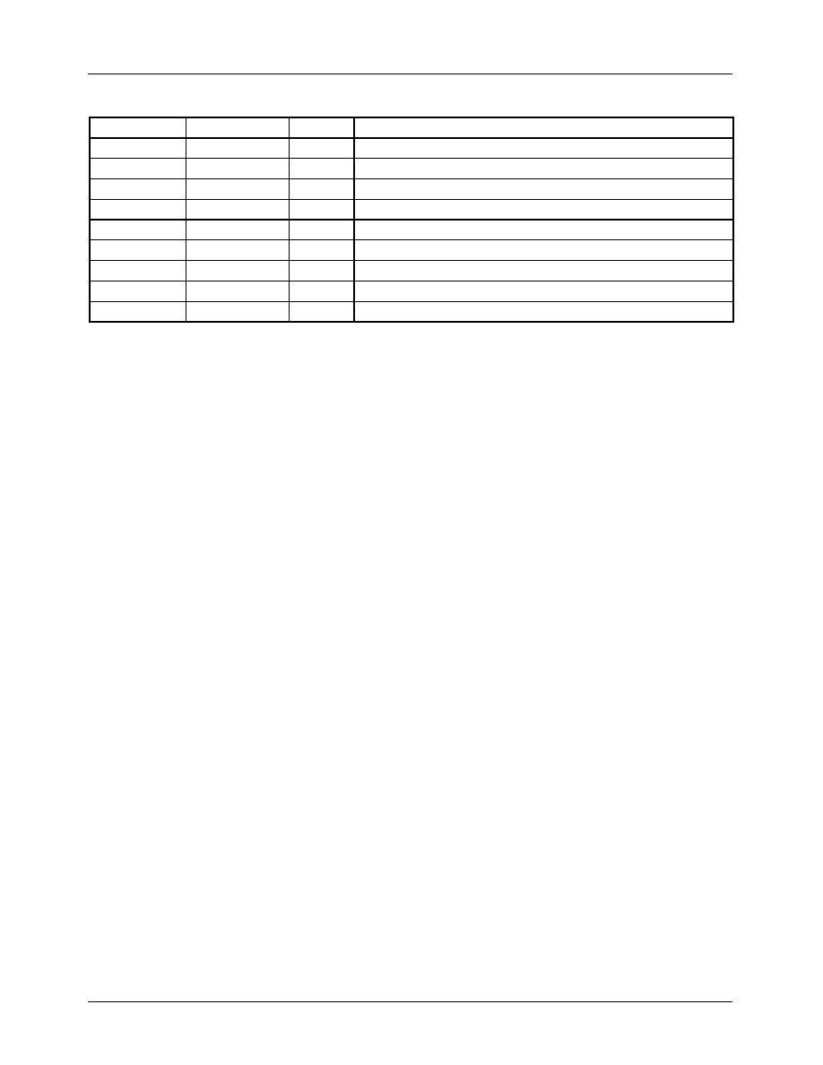
Pin Definitions (Continued)
Pin Number
Pin Name
I/O
Pin Function Description
40
OPOUT
O
Opamp output
41
OPIN(
-
)
I
Opamp input (
-
)
42
OPIN(+)
I
Opamp input (+)
43
RES50
I
Regulator 5V reset
44
SVCC
-
Signal supply voltage
45
REF
I
Bias voltage input
46
REG050
O
Regulator 5V output
47
REG50
O
Regulator output
48
IN1.1
I
CH 1 opamp input (+)
KA3031
5
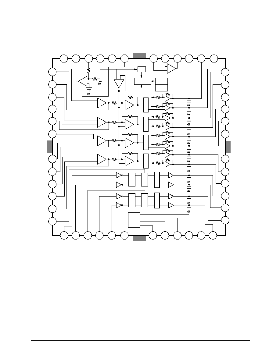
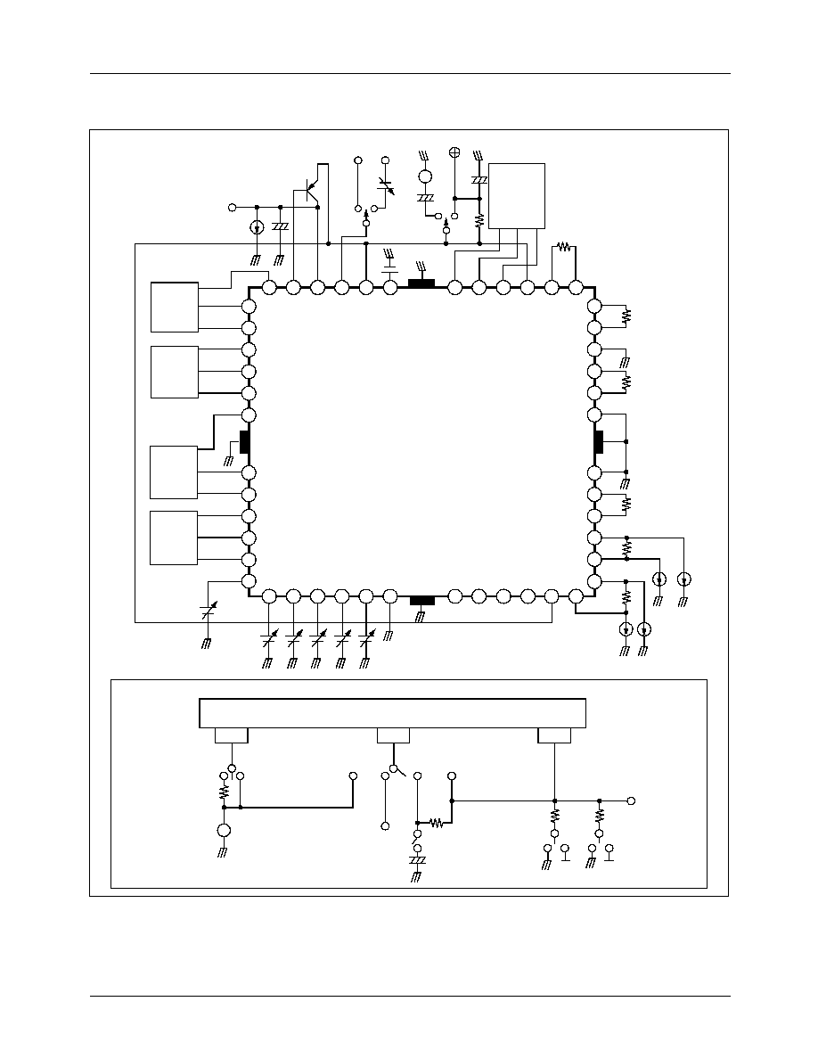
Internal Block Diagram
Notes:
1. SW = Logic switch
2. MSC = Motor speed control
3. D = Output driver
+
-
+
-
+
-
+
-
+
-
+
-
+
-
+
-
-
+
+
-
-
+
-
+
-
+
-
+
-
+
-
+
-
+
-
+
-
+
-
+
-
+
S
W
S
W
M
S
C
M
S
C
-
+
-
+
D
D
D
D
MUTE4
MUTE3
MUTE2
MUTE1
ALL MUTE
SW
T.S.D
O.V.P
1
2
3
4
5
6
7
8
9
10
11
12
13
14
15
16
17
18
19
20
21
22
23
24
25
26
27
28
29
30
31
32
33
34
35
36
37
38
39
40
41
42
43
44
45
46
47
48
+
-
2P
2P
2P
2P
2P
2P
2P
2P
2P
2P
2P
2P
2.5V
IN1.2
OUT1
IN2.1
IN2.2
OUT2
IN3.1
IN3.2
OUT3
IN4.1
IN4.2
OUT4
CTL1
DO2.1
DO2.2
PGND3
DO3.1
DO3.2
PGND2
PGND1
DO4.1
DO4.2
DO5.1
DO5.2
DO6.1
FWD1
REV1
CTL
FWD2
REV2
SGND
MUTE1 MUTE2 MUTE3 MUTE4 PVCC1 DO6.2
DO1.2
DO1.1
PVCC2
OPOUT
OPIN(
-
)
OPIN(+)
RES50
SVCC
REF
REG050
REG50
IN1.1
KA3031
6
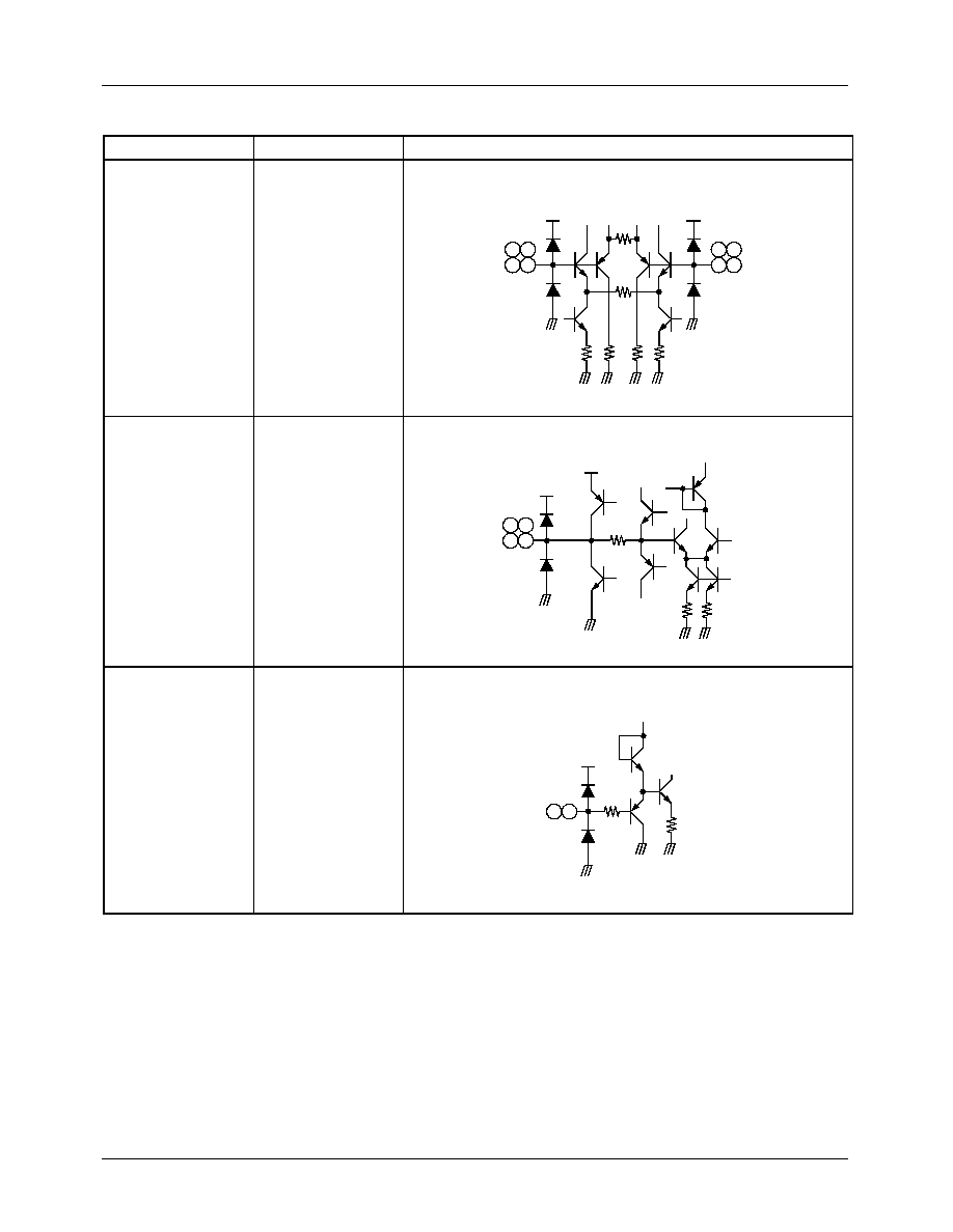
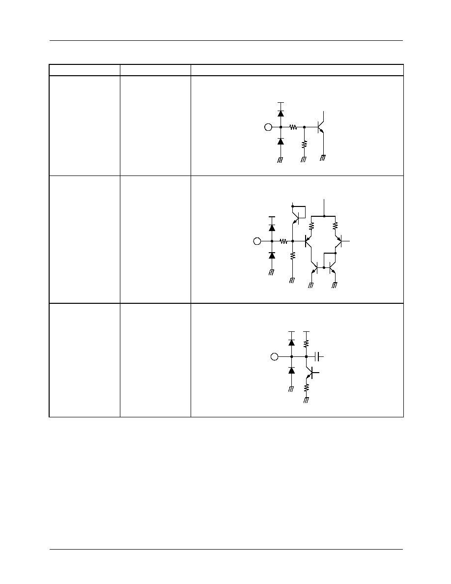
Equivalent Circuits
Description
Pin No.
Internal circuit
Input
OPIN (+)
OPIN (
-
)
48, 3, 6, 9
1, 4, 7. 10
Input
opout
2, 5, 8, 11
CTL
12, 15
VCC
VCC
10k
4k
10k
48 3
6 9
1 4
7 10
VCC
VCC
2 5
8 11
10k
25k
Vr
VCC
0.1k
100k
12 15
KA3031
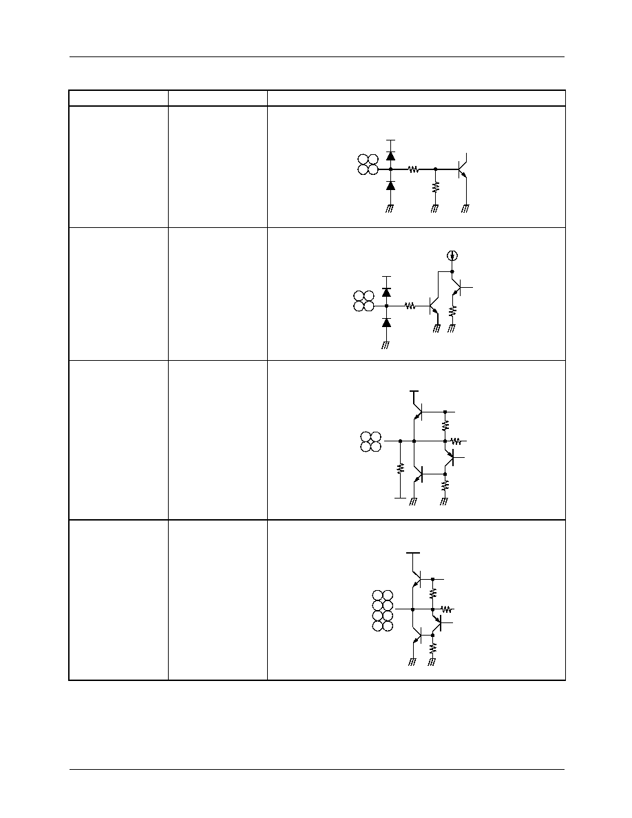
7
Equivalent Circuits (Continued)
Description
Pin No.
Internal circuit
Logic drive
FWD input
REV input
13, 16
14, 17
CH mute
19, 20
21, 22
Logic
drive
output
24, 25
26, 27
4-CH
drive
output
28, 29
32, 33
35, 36
37, 38
VCC
13 6
14 17
30k
30k
VCC
19 20
21 22
30k
2k
24 25
26 27
1k
20k
VCC
Vr
1k
10k
28 29
32 33
35
37 38
36
10k
1k
VCC
10k
KA3031
8
Equivalent Circuits (Continued)
Description
Pin No.
Internal circuit
Normal
opout
40
Normal
OPIN(+)
OPIN(
-
)
42
41
Ref
45
VCC
VCC
40
50
50
41
VCC
VCC
42
5k
VCC
45
2k
0.1k
KA3031
9
Equivalent Circuits (Continued)
Description
Pin No.
Internal circuit
RES50
43
REG050
46
REG50
47
50k
50k
VCC
43
10k
VCC
2k
2k
10k
41
VCC
53k
VCC
47
10k
KA3031
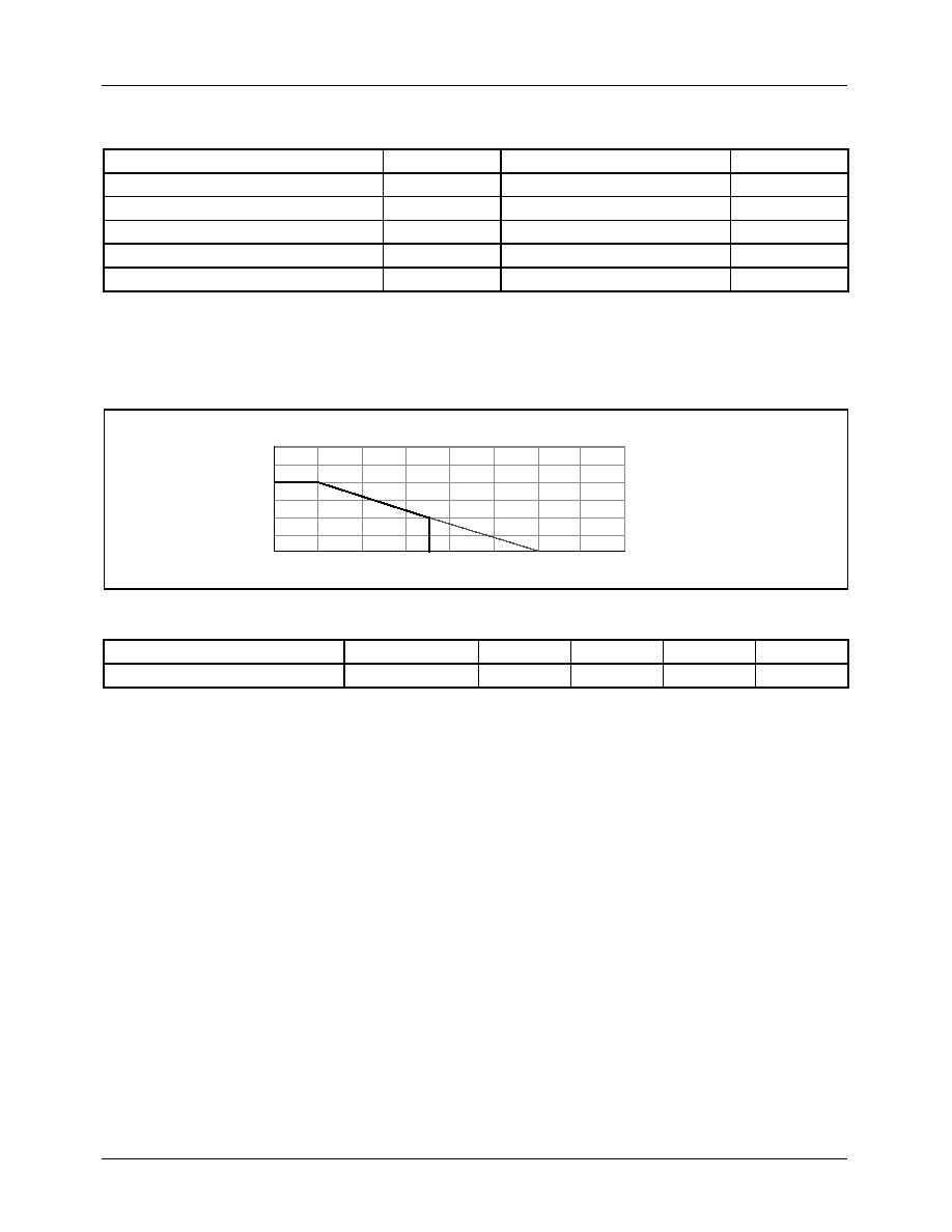
10
Absolute Maximum Ratings
(Ta = 25
°
°
°
°
C)
NOTE:
1. When mounted on 70mm
×
70mm
×
1.6mm PCB.
2. Power dissipation reduces 16mW /
°
C for using above Ta=25
°
C.
3. Do not exceed Pd and SOA.
Power Dissipation Curve
Recommended Operating Conditions
(Ta = 25
°
°
°
°
C)
Parameter
Symbol
Value
Unit
Maximum supply voltage
V
CC
18
V
Power dissipation
P
D
3
note
W
Operating temperature
T
OPR
-
35 ~ +85
°
C
Storage temperature
T
STG
-
55 ~ +150
°
C
Maximum output current
I
OMAX
1
A
Parameter
Symbol
Min.
Typ.
Max.
Unit
Operating supply voltage
V
CC
4.5
-
16
V
3,500
2,500
1,500
0
0
25
50
75
100
125
150
175
Pd (mW)
Ambient temperature, Ta [
°
C]
KA3031
11
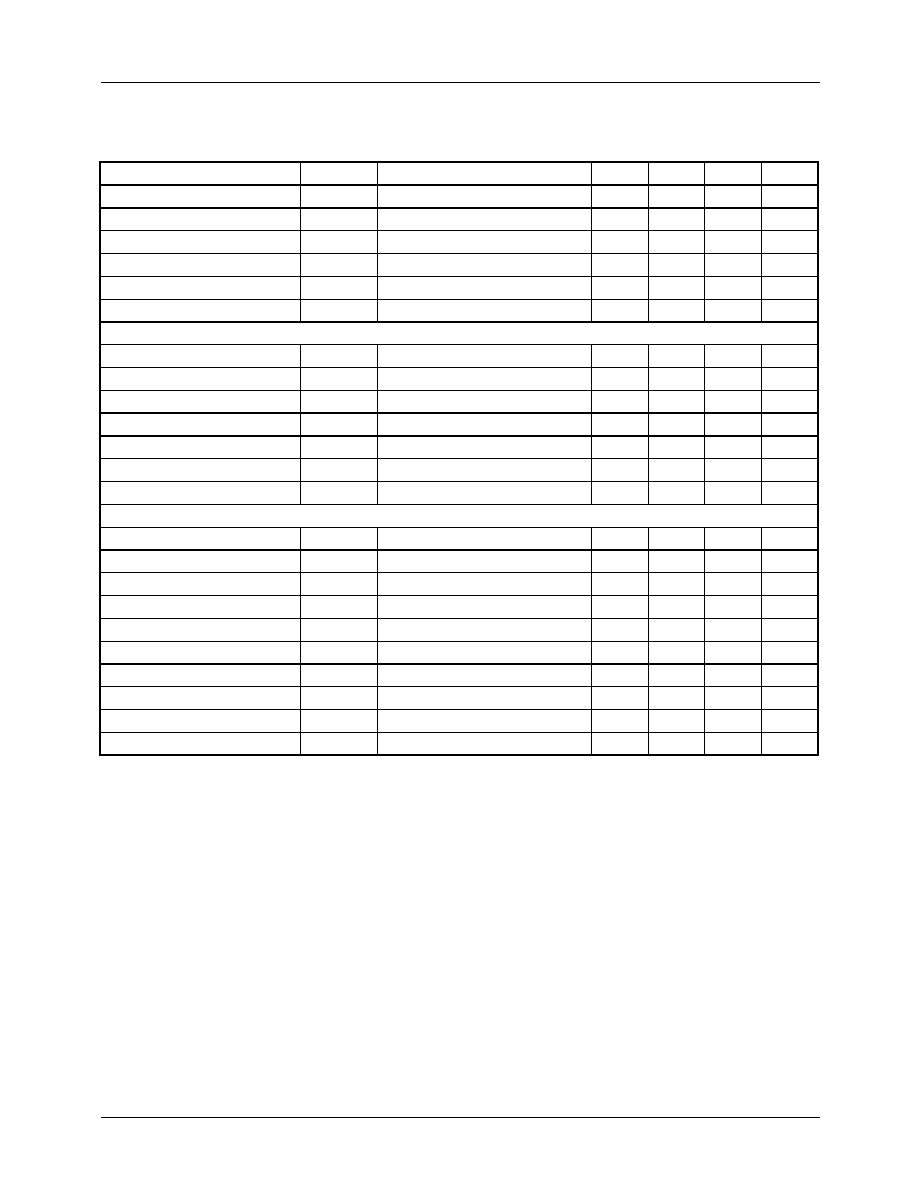
Electrical Characteristics
(SV
CC
=PV
CC1
=PV
CC2
=8V, Ta=25
°
C, unless otherwise specified)
Parameter
Symbol
Conditions
Min.
Typ.
Max.
Units
Quiescent circuit current
I
CC
under no-load
9
12
16
mA
All mute on current
I
MUTE ALL
Pin 45=GND
-
6
10
mA
All mute on voltage
V
MON ALL
Pin 45=Variation
-
-
0.5
V
All mute off voltage
V
MOFF ALL
Pin 45=Variation
2
-
-
V
CH mute on voltage
V
MON CH
Pin 19, 20, 21, 22=Variation
2
-
-
V
CH mute off voltage
V
MOFF CH
Pin 19, 20, 21, 22=Variation
-
-
0.5
V
DRIVER PART (R
L
=8
)
Input offset voltage
V
IO
-
-
20
-
+20
mV
Output offset voltage
V
OO
V
IN
=2.5V
-
50
-
+50
mV
Maximum output voltage 1
V
OM1
V
CC
=8V, R
L
=8
4.0
5.5
-
V
Maximum output voltage 2
V
OM2
V
CC
=13V, R
L
=24
7
9
-
V
Closed-loop voltage gain
A
VF
V
IN
=0.1V
RMS
9
10.5
12
dB
Ripple rejection ratio
RR
V
IN
=0.1V
RMS
, f=120kHz
-
50
-
dB
Slew rate
SR
Square, Vout=2Vp-p, f=120kHz
-
0.8
-
V/
µ
s
NORMAL OPAMP PART
Input offset voltage
V
OF1
-
-
10
-
+10
mV
Input bias current
I
B1
-
-
-
300
nA
High level output voltage
V
OH1
R
L
=50
6
6.8
-
V
Low level output voltage
V
OL1
R
L
=50
-
1.0
1.8
V
Output sink current
I
SINK1
V
IN
=
-
75dB, f=1kHz
10
40
-
mA
Output source current
I
SOURCE1
V
IN
=
-
20dB, f=120kHz
10
40
-
mA
Open loop voltage gain
GV
O1
Square, Vout=2Vp-p, f=120kHz
-
75
-
dB
Ripple rejection ratio
RR1
V
IN
=
-
20dB, f=1kHz
-
65
-
dB
Slew rate
SR1
-
-
1
-
V/
µ
s
Common mode rejection ratio
CMRR1
-
-
80
-
dB
KA3031
12
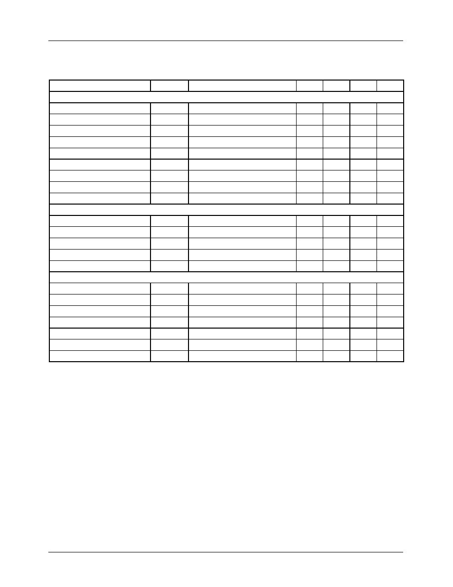
Electrical Characteristics (Continued)
(SV
CC
=PV
CC1
=PV
CC2
=8V, Ta=25
°
C, unless otherwise specified)
Parameter
Symbol
Conditions
Min.
Typ.
Max.
Units
INPUT OPAMP PART
Input offset voltage
V
OF2
-
-
10
-
+10
mV
Input bias current
I
B2
-
-
-
400
nA
High level output voltage
V
OH2
-
7
7.7
-
V
Low level output voltage
V
OL2
-
-
0.2
0.5
V
Output sink current
I
SINK2
-
500
800
-
µ
A
Output source current
I
SOURCE2
-
500
800
-
µ
A
Open loop voltage gain
GV
O2
V
IN
=
-
75dB, f=1kHz
-
80
-
dB
Slew rate
SR2
Square, Vout=2Vp-p, f=120kHz
-
1
-
V/
µ
s
Common mode rejection ratio
CMRR2
V
IN
=
-
20dB, f=1kHz
-
80
-
dB
5V REGULATOR PART
Regulator output voltage
Vreg
I
L
=100mA
4.75
5
5.25
V
Load regulation
V
R1
I
L
=0
200mA
-
40
0
+10
mV
Line regulation
V
CC
I
L
=200mA, V
CC
=6V
9V
-
20
0
+30
mV
Reset on voltage
Reson
-
-
-
0.5
V
Reset off voltage
Resoff
-
2
-
-
V
TRAY, CHANGER DRIVER PART (R
L
=45
)
Input high level voltage
V
IH
-
2
-
-
V
Input low level voltage
V
IH
-
-
-
0.5
V
Output voltage 1
V
O1
V
CC
=8V, V
CTL
=3.5V
5.2
6.0
6.8
V
Output voltage 2
V
O2
V
CC
=13V, V
CTL
=4.5V
7.5
8.5
9.5
V
Output load regulation
V
R1
-
-
300
700
mV
Output offset voltage 1
V
OO1
V
IN
=5V, 5V
-
10
-
+10
mV
Output offset voltage 2
V
OO2
V
IN
=0V, 0V
-
10
-
+10
mV
KA3031
13
Application Information
1. REFERENCE INPUT & ALL MUTE FUNCTION
Pin 45 (REF) can use the reference Input pin or the all mute signal input pin.
· Reference input
In the case of the reference input pin, you must keep the applied voltage range between 2[V] and 6.5[V] at
V
CC
= 8[V].
· All mute input
When using the all mute function pin, applied voltage condition is as follows.
2. SEPARATED CHANNEL MUTE FUNCTION
These pins are used for individual channel mute operation.
· When the mute pins (pin19, 20, 21 and 22) are high level, the mute circuits are activated so that the output circuit is muted.
· When the voltage of the mute pins (pin19, 20, 21 and 22) are low level, the mute circuit is stopped and output circuits
operate normally.
· If the chip temperature rises above 175
°
C, then the thermal shutdown (TSD) circuit is activated and the output circuits are
muted.
- Mute 1 (pin 19)-CH1 mute control input pin.
- Mute 2 (pin 20)-CH2 mute control input pin.
- Mute 3 (pin 21)-CH3 mute control input pin.
- Mute 4 (pin 22)-CH4 mute control input pin.
3. PROTECTION FUNCTION
· Thermal shutdown (TSD)
If the chip temperature rises above 175
°
C, then the thermal shutdown (TSD) circuit is activated and the output circuit is will
be mute. The TSD circuit is temperature hysteresis 25
°
C.
· Under voltage lockout (UVLO) and over voltage protection (OVP)
It is designed to mute-operate the internal bias by the function of UVLO and OVP, when the power supply voltage falls
below 3.5[V] or above 20[V].
All mute on voltage
Below 0.5[V]
Mute function operation
All mute off voltage
Above 2[V]
Normal operation
KA3031
14
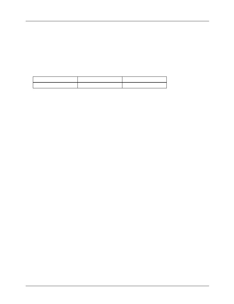
4. REGULATOR & RESET FUNCTION
The regulator and reset circuits are as illustrated in Figure 1.
where R1=R2.
· The external circuit is composed of the transistor, KSB772 and a capacitor, about 33[
µ
F]. The capacitor is used as a ripple
eliminator and should have good temperature characteristics.
· The regulator output voltage (pin 46) is decided as follows.
Vout = 2
×
2.5 = 5[V] (where R1 = R2)
· When the voltage of pin 43 (Vreset) is at 5[V], the regulator output voltage (pin 46) because 5[V]. If the voltage
of pin 43 is 0[V], the output voltage of pin 46 because 0[V].
Figure 1. Regulator circuit
+
-
39
43
44
46
47
KSB772
REG OUT
V
CC
33
µ
F
2.5V
R1
R2
Vreset
+
KA3031
KA3031
15
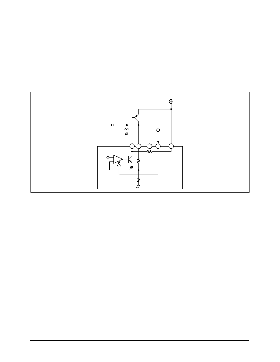
5. FOCUS, TRACKING ACTUATOR, SPINDLE, SLED MOTOR DRIVE PART
· The voltage, Vref is the reference voltage given by the external bias voltage of the pin 45.
· The input signal (Vin) through pins 3, 6, 9 and 48 is amplified one times (Rref1 = Rfeed1) by the AP1 and then fed to the
level shift.
· The level shift produces the current due to the difference between the input signal and the arbitrary reference signal. The
current produced as +
I and
-
I are fed into the output amplifier, where output amplifier (AP2, 3) gain is two times (all
Rref2 = Rfeed2).
· If you desire to change the gain, the input buffer amplifier (BF) can be used.
· The output stage is the balanced transformerless (BTL) driver.
· The bias voltage Vr is expressed as below;
+
-
+
-
+
-
+
+
-
M
45
2
5
8 11
1
4
7 10
3
6
9 48
Vin
BF
Vref
Rref1
AP1
Rfeed1
+
-
LEVEL
SHIFT
Rref2
IC
Vr
Rref2
AP2
AP3
Rfeed2
Rfeed2
-
Vr
V
CC
V
BE
2
----------------------------
V
[ ]
=
KA3031
16
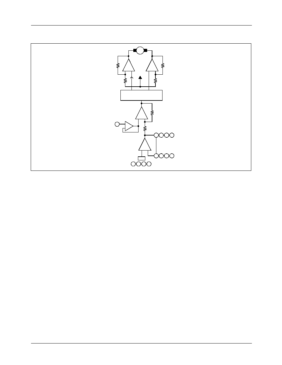
6. TRAY, CHANGE MOTOR DRIVE PART
· Rotational direction control
The forward and reverse rotational direction is controlled by FWD (pin 13, 16) and REV (pin 14, 17) input conditions are as
follows.
· where Vr is (Vcc - Vbe) / 2 = 3.65V (at Vcc=8V)
· where Out1 pins are pins 24 and 26, and out2 pins aer pins 25 and 27
· Motor speed control
- The almost maximum torque is obtained when it is used with the pins 12 and 15 (CTL1, 2) open.
- If the torque of the motor is too low, then the applied voltage at pins 12 and 15 (CTL1, 2) are 0[V].
- When motor speed controlled, the applied voltage of the pins 12 and 15 (CTL1, 2) is between 0 and 4V.
Also, if the speed control is constant, the applied voltage of the pins 12 and 15 (CTL1, 2) is between 4 and
5V.
- This IC's applied maximum voltage is 6V when V
CC
is 8V.
- You must not use the applied CTL1, 2 voltage above 5.8V when V
CC
is 8V, and 3V when V
CC
is 5V.
INPUT
OUTPUT
FWD
REV
OUT 1
OUT 2
State
H
H
Vr
Vr
Brake
H
L
H
L
Forward
L
H
L
H
Reverse
L
L
Vr
Vr
Brake
M
24
26
25
27
12
15
13
16
14
17
out 1
out 2
D
LEVEL SHIFT
M.S.C
S.W
D
CTL1, 2
IN
FWD
REV
IN
KA3031
17
Typical Performance Characteristics
Total circuit
Focus, Tracking, Spindle, Sled drive part
11
11.5
12
12.5
13
13.5
14
5
6
7
8
9
10
11
12
13
14
Icc(mA)
Icc(mA)
Vcc(V)
<Vcc vs Icc>
Vcc=Var.
Temp=25
°
C
11.4
11.6
11.8
12.2
12.4
12.6
12.8
13.0
12.0
13.2
13.4
Temp(
°
C)
<Temp vs Icc>
Vcc=8V
Temp= Var.
-30
-10
0
10
30
40
50
60
70
80
V
IN
(V)
Temp(
°
C)
Vom(V)
0.0
1.0
2.0
3.0
4.0
5.0
6.0
7.0
8.0
9.0
10.0
4
5
6
7
8
9
10
11
12
13
<Vcc vs Vom>
Vcc=Vari.
Temp=25
°
C
RL=8
Vcc(V)
0.0
2.0
4.0
6.0
8.0
10.0
12.0
4
5
6
7
8
9
10
11
12
13
Avf(dB)
Avf(dB)
<Vcc vs Avf>
Vcc=Var.
Temp=25
°
C
RL=8
Vin=0.1Vrms
f=1KHz
Vcc(V)
0.0
0.5
1.0
1.5
2.0
2.5
3.0
3.5
4.0
4.5
5.0
0.2
0.4
0.6
0.8
1
12
14
Vout(V)
<Vin vs Vout>
Vcc=8V
Temp=25
°
C
RL=8
Vin= Var.
10.3
10.4
10.5
10.6
10.7
10.8
10.9
Vcc=8V
temp= Var.
RL=8
Vin=0.1Vrms
f=1KHz
<Temp vs Avf>
-30
-10
0
10
30
40
50
60
70
80
KA3031
18
Typical Performance Characteristics (Continued)
Tray, Change drive part
Vom(V)
5.32
5.34
5.36
5.38
5.42
5.44
5.46
5.48
5.50
5.40
5.52
<Temp vs Vom>
Temp (
°
C)
Vcc=8V
temp= Var.
RL=8
-30
-10
0
10
30
40
50
60
70
80
Temp (
°
C)
0.0
1.0
2.0
3.0
4.0
5.0
6.0
7.0
8.0
9.0
4
5
6
7
8
9
10
11
12
13
Vo (V)
<Vcc vs Vo>
Vcc=Var.
Temp=25
°
C
RL=45
Vin=5V/0V
Vctl=3.5V
Vcc(V)
5.4
5.5
5.6
5.7
5.8
5.9
6.0
6.1
Vo (V)
<Temp vs Vo>
Vcc=8V
temp= Var.
RL=45
Vin=5V/0V
Vctl=3.5V
Vo (V)
0.0
1.0
2.0
3.0
4.0
5.0
6.0
7.0
0.5
1
1.5
2
2.5
3
3.5
4
4.5
5
<Vctl vs Vo>
Vcc=8V
Temp=25
°
C
RL=45
Vin= 5V/0V
Vctl= Var.
Vctl(V)
Vo (V)
0.0
1.0
2.0
3.0
4.0
5.0
6.0
7.0
0.5
1
1.5
2
2.5
3
3.5
4
4.5
5
<Vctl vs Vo>
Vcc=8V
Temp=25
°
C
RL=8
Vin= 5V/0V
Vctl= Var.
Vctl(V)
-30
-10
0
10
30
40
50
60
70
80
KA3031
19
Typical Performance Characteristics (Continued)
Regulator part
Normal Op Amp part
0.0
1.0
2.0
3.0
4.0
5.0
6.0
4
5
6
7
8
9
10
11
12
13
<Vcc vs Vreg>
<Temp vs Vreg>
Vcc=Var.
Temp=25
°
C
IL=100mA
Vcc(V)
4.94
4.96
4.98
5.00
5.02
5.04
5.06
5.08
- 30
- 10
0
10
30
40
50
60
70
80
Temp (
°
C)
Vreg (V)
Vreg (V)
Vcc=8V
Temp=Var.
IL=100mA
4
5
6
7
8
9
10
11
12
13
-30
-10
0
10
30
40
50
60
70
80
Temp (
°
C)
0.0
10.0
20.0
30.0
40.0
50.0
60.0
70.0
Isou1(mA)
Isou1(mA)
Isink1(mA)
<Vcc vs Isource>
<Temp vs Isource>
<Vcc vs Open loop voltage gain>
<Vcc vs Isink>
0.0
10.0
20.0
30.0
40.0
50.0
60.0
70.0
4
5
6
7
8
9
10
11
12
13
Vcc(V)
68.0
70.0
72.0
74.0
76.0
78.0
80.0
82.0
84.0
86.0
4
5
6
7
8
9
10
11
12
13
GVo1(dB)
Vcc(V)
Vcc(V)
51.0
52.0
53.0
54.0
55.0
56.0
57.0
58.0
59.0
Vcc=8V
Temp=Var.
RL=50
Vcc=Var.
Temp=25
°
C
RL=50
Vcc=Var.
Temp=25
°
C
RL=1K
Vin=100uVp_p
f=1KHz
Vcc=Var.
Temp=25
°
C
RL=50
KA3031
20
Typical Performance Characteristics (Continued)
Input Op Amp part
0.0
10.0
20.0
30.0
40.0
50.0
60.0
-30
-10
0
10
30
40
50
60
70
80
Temp (
°
C)
Vcc=8V
temp=VAR
RL=50
<Temp vs Isink>
Isink1(mA)
0
500
1000
1500
2000
2500
4
5
6
7
8
9
10
11
12
13
Isou2(uA)
Isink2(uA)
Vcc(V)
Vcc(V)
Vcc(V)
<Vcc vs Isource>
<Vcc vs Isink>
0
200
400
600
800
1000
1200
1400
1600
4
5
6
7
8
9
10
11
12
13
73
74
75
76
77
78
79
80
81
82
83
4
5
6
7
8
9
10
11
12
13
<Vcc vs Open loop voltage gain>
GVo2(uA)
Vcc=Var.
Temp=25
°
C
RL=1K
Vcc=Var.
Temp=25
°
C
RL=1K
Vcc=Var.
Temp=25
°
C
RL=1K
KA3031
21
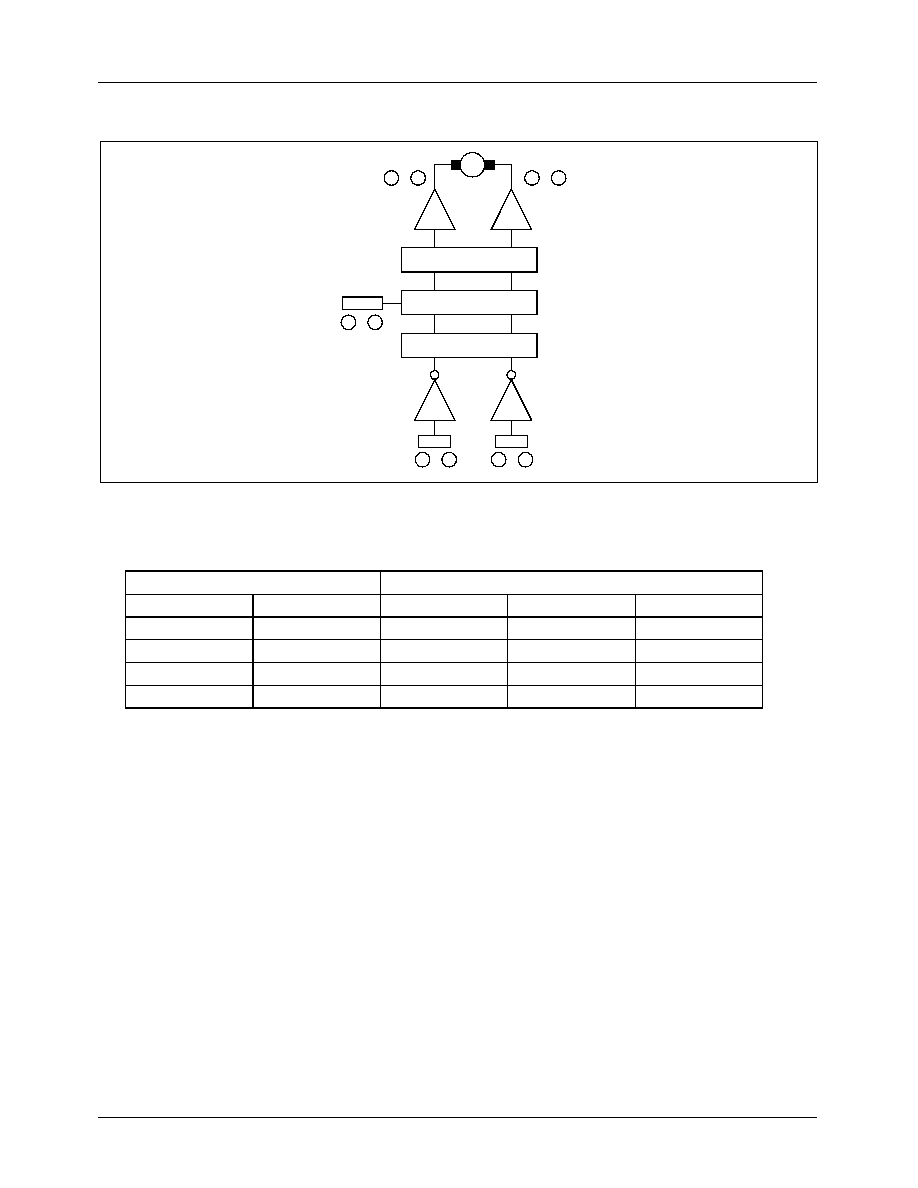
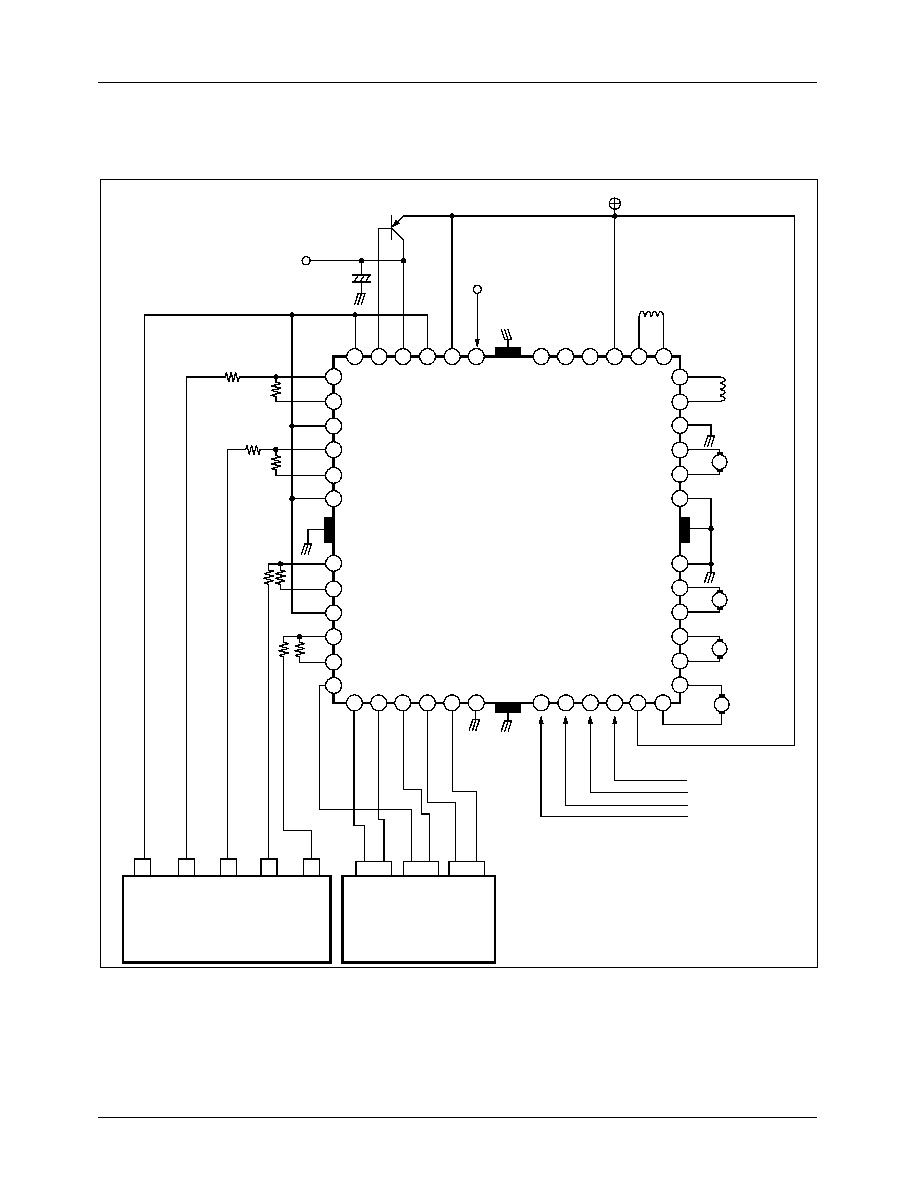
Test Circuits
37
38
39
40
41
42
43
44
45
46
47
48
9
10
11
12
8
7
6
5
4
1
2
3
13
14
15
16
17
18
19
20
21
22
23
24
25
26
27
28
29
30
31
32
33
34
35
36
OPIN (+)
OPIN (
-
)
OPOUT
OPIN (+)
OPIN (
-
)
OPOUT
OPIN (+)
OPIN (
-
)
OPOUT
OPIN (+)
OPIN (
-
)
OPOUT
O
P
I
N
(+
)
O
P
I
N
(
-
-
-
-
)
O
P
O
U
T
KSB772
REG OUT
+
IL
33
µ
F
Vreset
SW1
Ripple
All
V
CC
Vref
2.5V mute
2
1
20
RL
RL
RL
IL
RL
RL
IL
IL
IL
IN1A IN1B CTL2 IN2A IN2B
CTL1
~
RL
100
µ
F
+
+
1000
µ
F
1
2
OPIN(+)
OPIN(
-
)
OPOUT
SW3
SW7
SW5
SW6
1
2
V
CC
A
1M
~
V
CC
2
1
1M
B
D
50
1k
1
2
3
4
10
µ
F
opamp part
1
2
1
KA3031
IN1.2
OUT1
IN2.1
IN2.2
OUT2
IN3.1
IN3.2
OUT3
IN4.1
IN4.2
OUT4
CTL1
FW
D1
REV1
CTL
FW
D2
REV2
SGND
MUTE1
MUTE2
MUTE3
MTUE4
PVCC1
DO6.
2
DO6.1
DO5.2
DO5.1
DO4.2
DO4.1
PGND1
PGND2
DO3.2
DO3.1
PGND3
DO2.2
DO2.1
IN
1
.
1
RE
G
5
0
REG0
50
REF
SVCC
RES
5
0
OP
I
N
(
+
)
OPI
N
(
-
)
OPOUT
PVCC2
DO1.
1
DO1.
2
KA3031
22
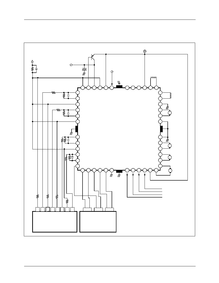
Application Circuits
Voltage Mode Control
Notes:
Radiation pin is connected to the internal GND of the package.
Connect the pin to the external GND.
1
2
3
4
5
6
7
8
9
10
11
12
13
14
15
16
17
18
19
20
21
22
23
24
25
26
27
28
29
30
31
32
33
34
35
36
37
38
39
40
41
42
43
44
45
46
47
48
KSB772
REG OUT
Vreset
33
µ
F
+
VCC
TRACKING
FOCUS
SPINDLE
SLED
TRAY
CHANGE
M
M
M
M
SLED MUTE
SPINDLE MUTE
TRACKING MUTE
FOCUS MUTE
TRAT
INPUT
CONTROL
TY CG
CHANGE
INPUT
REF &
ALL
MUTE
FOCUS
INPUT
TRACKING
INPUT
SPINDLE
INPUT
SLED
INPUT
[SERVO PRE AMP]
[CONTROLLER]
Where TY is tray motor.
CG is change motor
KA3031
IN
1
.
1
REG50
REG050
RE
F
SV
CC
RES50
OPI
N
(
+
)
OPI
N
(
-
)
OPOU
T
PVCC2
DO1.
1
DO1.
2
IN1.2
OUT1
IN2.1
IN2.2
OUT2
IN3.1
IN3.2
OUT3
IN4.1
IN4.2
CTL1
OUT4
DO6.1
DO5.2
DO5.1
DO4.2
DO4.1
PGND1
PGND2
DO3.2
DO3.1
PGND3
DO2.2
DO2.1
FW
D1
REV1
CTL
FW
D2
REV2
SGND
MUTE1
MUTE2
MUTE3
MTUE4
PVCC1
DO6
.
2
KA3031
23
Application Circuits
Differential Mode Control
1
2
3
4
5
6
7
8
9
10
11
12
13
14
15
16
17
18
19
20
21
22
23
24
25
26
27
28
29
30
31
32
33
34
35
36
37
38
39
40
41
42
43
44
45
46
47
48
KSB772
REG OUT
Vreset
33
µ
F
+
VCC
TRACKING
FOCUS
SPINDLE
SLED
TRAY
CHANGE
M
M
M
M
SLED MUTE
SPINDLE MUTE
TRACKING MUTE
FOCUS MUTE
TRAT
INPUT
CONTROL
TY CG
CHANGE
INPUT
[SERVO PRE AMP]
[CONTROLLER]
Where TY is tray motor.
CG is change motor
KA3031
REF &
ALL
MUTE
FOCUS TRACKING SPINDLE SLED
PWM1 PWM2 PWM3 PWM4 PWM5 PWM6 PWM7 PWM8
IN
1
.
1
RE
G50
REG0
50
REF
SVCC
RES
5
0
OP
I
N
(
+
)
OP
I
N
(
-
)
OPOUT
P
V
CC2
DO1.
1
DO1.
2
IN1.2
OUT1
IN2.1
IN2.2
OUT2
IN3.1
IN3.2
OUT3
IN4.1
IN4.2
CTL1
OUT4
DO6.1
DO5.2
DO5.1
DO4.2
DO4.1
PGND1
PGND2
DO3.2
DO3.1
PGND3
DO2.2
DO2.1
FW
D1
REV1
CTL
FW
D2
REV2
SGND
MUTE1
MUTE2
MUTE3
MTUE4
PVCC1
DO6
.
2

KA3031
12/1/00 0.0m 001
Stock#DSxxxxxxxx
2000 Fairchild Semiconductor International
LIFE SUPPORT POLICY
FAIRCHILD'S PRODUCTS ARE NOT AUTHORIZED FOR USE AS CRITICAL COMPONENTS IN LIFE SUPPORT DEVICES
OR SYSTEMS WITHOUT THE EXPRESS WRITTEN APPROVAL OF THE PRESIDENT OF FAIRCHILD SEMICONDUCTOR
INTERNATIONAL. As used herein:
1. Life support devices or systems are devices or systems
which, (a) are intended for surgical implant into the body,
or (b) support or sustain life, and (c) whose failure to
perform when properly used in accordance with
instructions for use provided in the labeling, can be
reasonably expected to result in a significant injury of the
user.
2. A critical component in any component of a life support
device or system whose failure to perform can be
reasonably expected to cause the failure of the life support
device or system, or to affect its safety or effectiveness.
www.fairchildsemi.com
DISCLAIMER
FAIRCHILD SEMICONDUCTOR RESERVES THE RIGHT TO MAKE CHANGES WITHOUT FURTHER NOTICE TO ANY
PRODUCTS HEREIN TO IMPROVE RELIABILITY, FUNCTION OR DESIGN. FAIRCHILD DOES NOT ASSUME ANY
LIABILITY ARISING OUT OF THE APPLICATION OR USE OF ANY PRODUCT OR CIRCUIT DESCRIBED HEREIN; NEITHER
DOES IT CONVEY ANY LICENSE UNDER ITS PATENT RIGHTS, NOR THE RIGHTS OF OTHERS.