 | –≠–ª–µ–∫—Ç—Ä–æ–Ω–Ω—ã–π –∫–æ–º–ø–æ–Ω–µ–Ω—Ç: KA311D | –°–∫–∞—á–∞—Ç—å:  PDF PDF  ZIP ZIP |
©2001 Fairchild Semiconductor Corporation
www.fairchildsemi.com
Rev. 1.0.1
Features
∑ Low input bias current : 250nA (Max)
∑ Low input offset current : 50nA (Max)
∑ Differential Input Voltage :
±
30V
∑ Power supply voltage : single 5.0V supply to
±
15V.
∑ Offset voltage null capability.
∑ Strobe capability.
Description
The KA311 series is a monolithic, low input current voltage
comparator. The device is also designed to operate from dual
or single supply voltage.
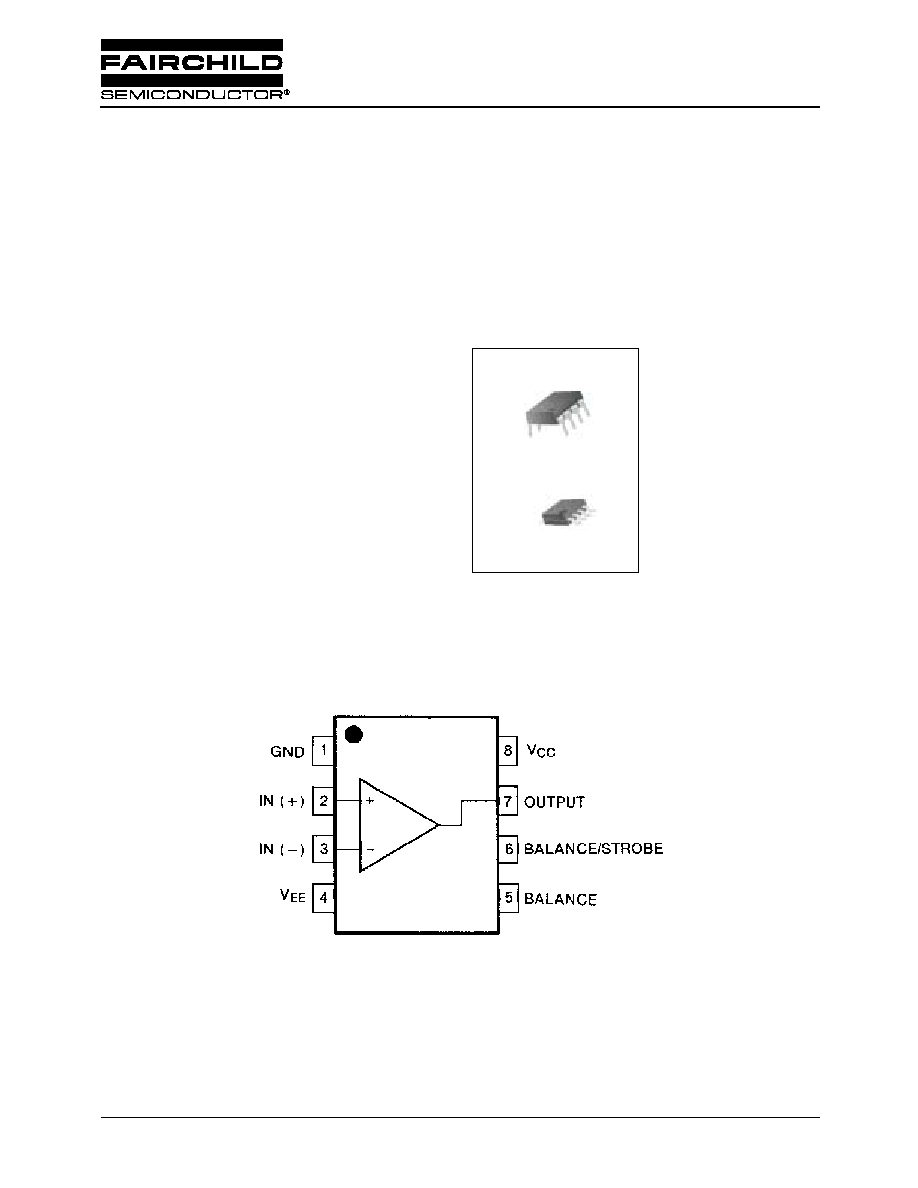
8-DIP
8-SOP
1
1
Internal Block Diagram
KA311
Single Comparator
KA311
2
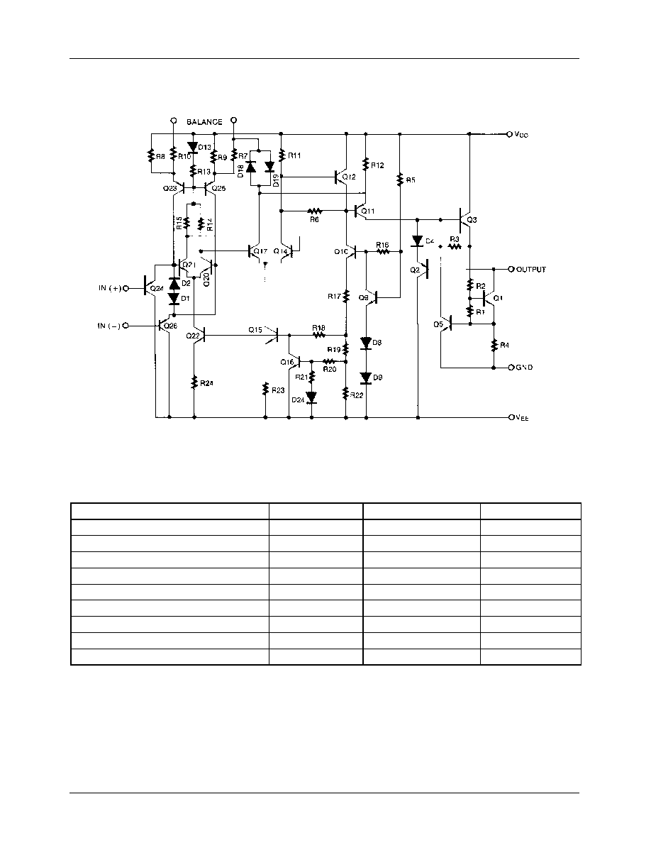
Schematic Diagram
Absolute Maximum Ratings
Parameter
Symbol
Value
Unit
Total Supply Voltage
V
CC
36
V
Output to Negative Supply Voltage KA311
V
O
- V
EE
40
V
Ground to Negative voltage
V
EE
-30
V
Differential Input Voltage
V
I(DIFF)
30
V
Input Voltage
V
I
±
15
V
Output Short Circuit Duration
-
10
sec
Power Dissipation
P
D
500
mW
Operating Temperature Range
T
OPR
0 ~ +70
∞
C
Storage Temperature Range
T
STG
- 65 ~ +150
∞
C
KA311
3
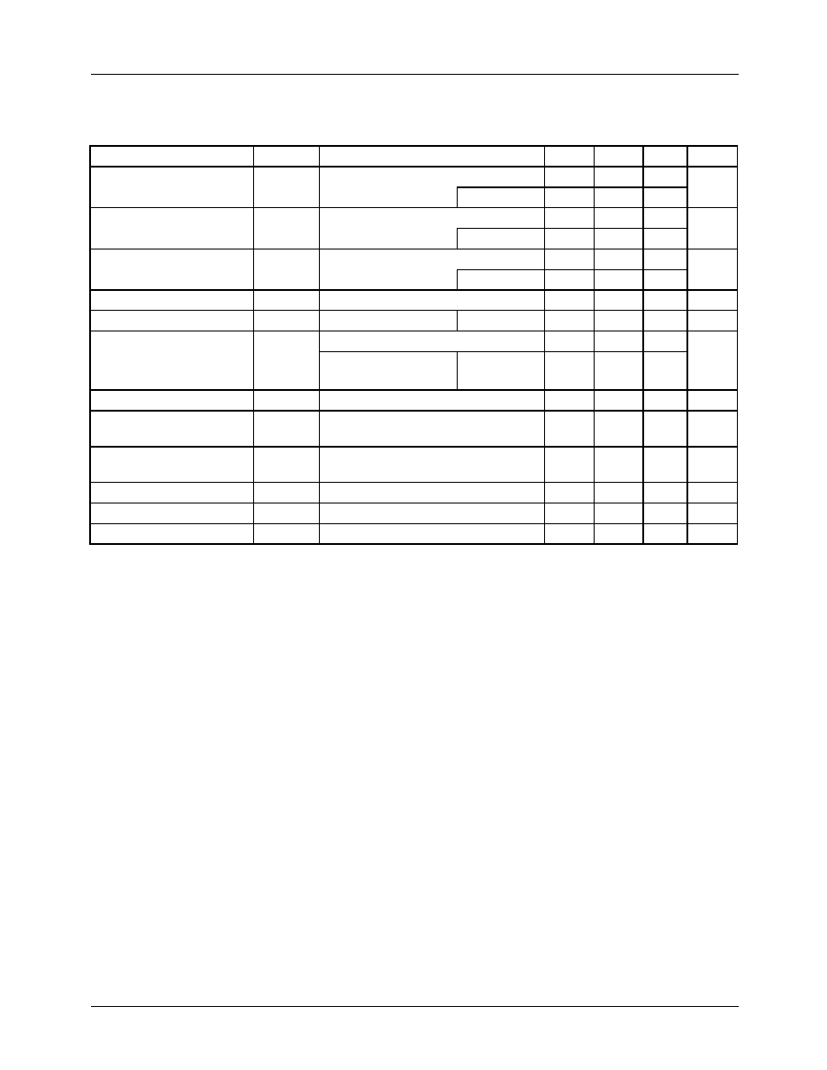
Electrical Characteristics
(V
CC
= 15V, T
A
= 25
∞
C, unless otherwise specified)
Notes :
1. 0
T
A
+70
∞
C
2. The response time specified is for a 100mV input step with 5mV over drive.
Parameter
Symbol
Conditions
Min.
Typ.
Max.
Unit
Input Offset Voltage
V
IO
R
S
50K
-
1.0
7.5
mV
Note 1
-
-
10
Input Offset Current
I
IO
-
6
50
nA
Note 1
-
-
70
Input Bias Current
I
BIAS
-
100
250
nA
Note 1
-
-
300
Voltage Gain
G
V
-
40
200
-
V/mV
Response Time
T
RES
Note 2
-
200
-
ns
Saturation Voltage
V
SAT
I
O
=50mA, V
I
-10mV
-
0.75
1.5
V
V
CC
4.5V, V
EE
=0V
I
O
=8mA, V
I
-10mV, Note 1
-
0.23
0.4
Strobe "ON" Current
I
STR(ON)
-
-
3
-
mA
Output Leakage Current
I
SINK
I
STR
=3mA, V
I
10mV
V
O
=15V, V
CC
=±15V
-
0.2
50
nA
Input Voltage Range
V
I(R)
Note 1
-14.5
to 13.0
-14.7
to 13.8
-
V
Positive Supply Current
I
CC
-
-
3.0
7.5
mA
Negative Supply Current
I
EE
-
-
-2.2
-5.0
mA
Strobe Current
I
STR
-
-
3
-
mA
KA311
4
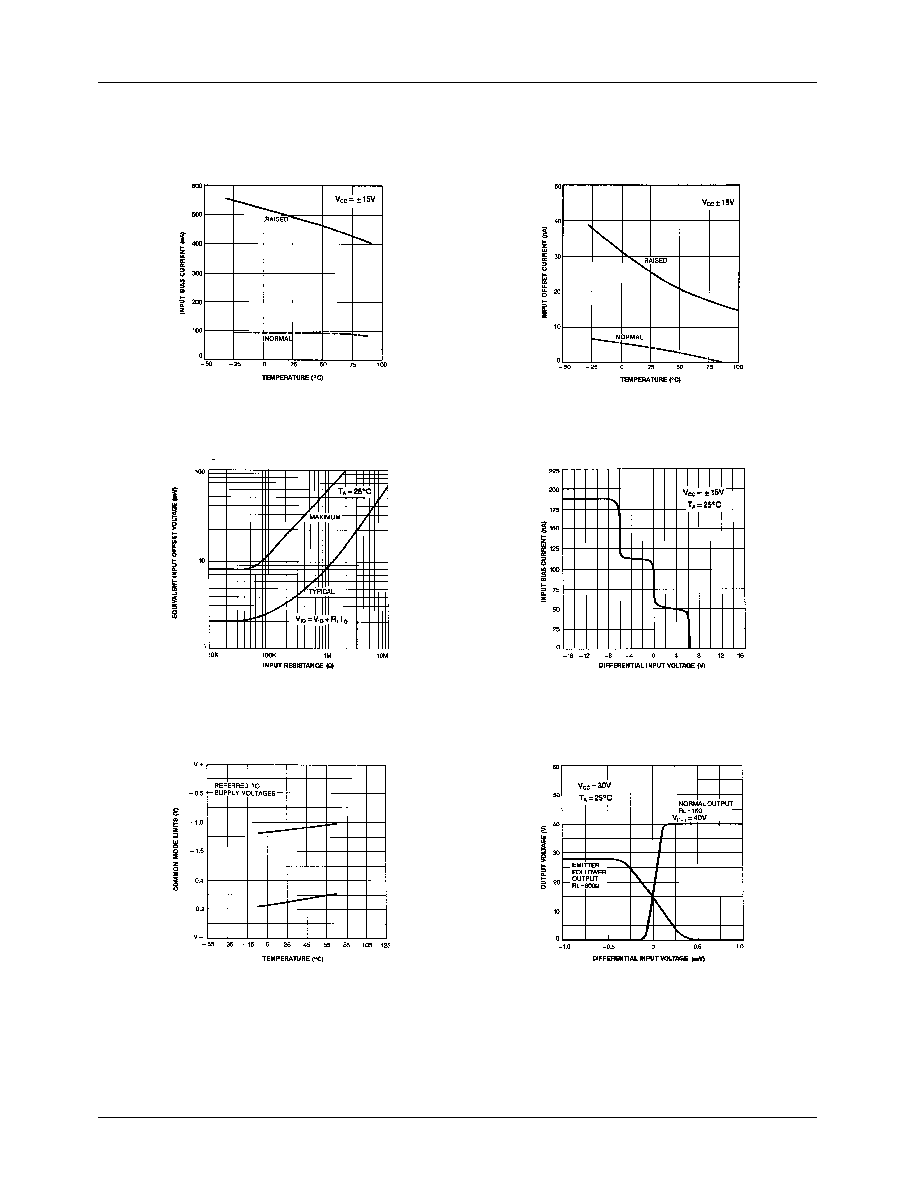
Typical Performance Characteristics
Figure 1. Input Bias Current vs Temperature
Figure 2. Input Offset Current vs Temperature
Figure 3. Offset Voltage vs Input Resistance
Figure 4. Input Bias Current vs
Differential input voltage
Figure 5. Common Mode Limits vs Temperature
Figure 6. Output Voltage vs
Differential input voltage
KA311
5
Typical Performance Characteristics (continued)
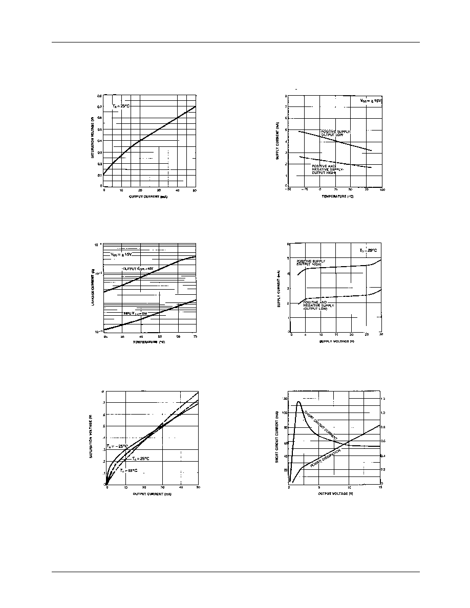
Figure 7. Saturation voltage vs Current
Figure 8. Supply Current vs Temperature
Figure 9. Leakage Current vs Temperature
Figure 10. Supply Current vs Supply Voltage
Figure 11. Current Saturation Voltage
Figure 12. Output Limiting Characterstics