 | ÐлекÑÑоннÑй компоненÑ: KA3511AS | СкаÑаÑÑ:  PDF PDF  ZIP ZIP |
KA3511BS Intelligent Voltage Mode PWM IC

©2001 Fairchild Semiconductor Corporation
www.fairchildsemi.com
Rev. 1.0.1
Features
· Complete PWM control and house keeping circuitry
· Few external components
· Precision voltage reference trimmed to 2%
· Dual output for push-pull operation
· Each output TR for 200mA sink current
· Variable duty cycle by dead time control
· Soft start capability by using dead time control
· Double pulse suppression logic
· Over voltage protection for 3.3V / 5V / 12V
· Under voltage protection for 3.3V / 5V / 12V
· One more external input for various protection (PT)
· Remote on/off control function (PS-ON)
· Latch function controlled by remote and protection input
· Power good signal generator with hysteresis
Precision reference section
The reference voltage trimmed to
±
2%
(4.9V
Vref
5.1V)
PG (Power good signal generator) section
Power good signal generator is to monitor the voltage level
of power supply for safe operation of a microprocessor.
KA3511BS requires few external components to accomplish
a complete housekeeping circuits for SMPS.
Description
The KA3511BS is a fixed frequency improved performance
pulse width modulation control circuit with complete
housekeeping circuitry for use in the secondary side of
SMPS (Switched mode power supply). It contains various
functions, which are precision voltage reference, over
voltage protection, under voltage protection, remote on/off
control, power good signal generator and etc.
OVP (Over voltage protection) section
It has OVP functions for +3.3V,+5V,+12V and PT outputs.
The circuit is made up of a comparator with four detecting
inputs and without hysteresis voltage. Especially, PT (Pin18)
is prepared for an extra OVP input or another protection
signal.
UVP (Under voltage protection) section
It also has UVP functions for +3.3V, +5V, +12V outputs. The
block is made up of a comparator with three detecting inputs
and without hysteresis voltage.
Remote on/off section
Remote on/off section is used to control SMPS externally. If
a high signal is supplied to the remote on/off input, PWM
signal becomes a high state and all secondary outputs are
grounded. The remote on/off signal is transferred with some
on-delay and off-delay time of 8ms, 24ms respectively.
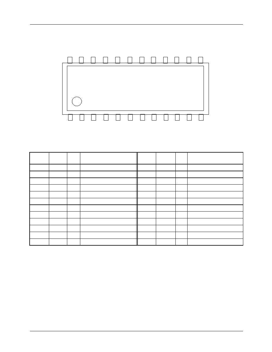
24-SDIP
1
KA3511BS
Intelligent Voltage Mode PWM IC
KA3511BS
2
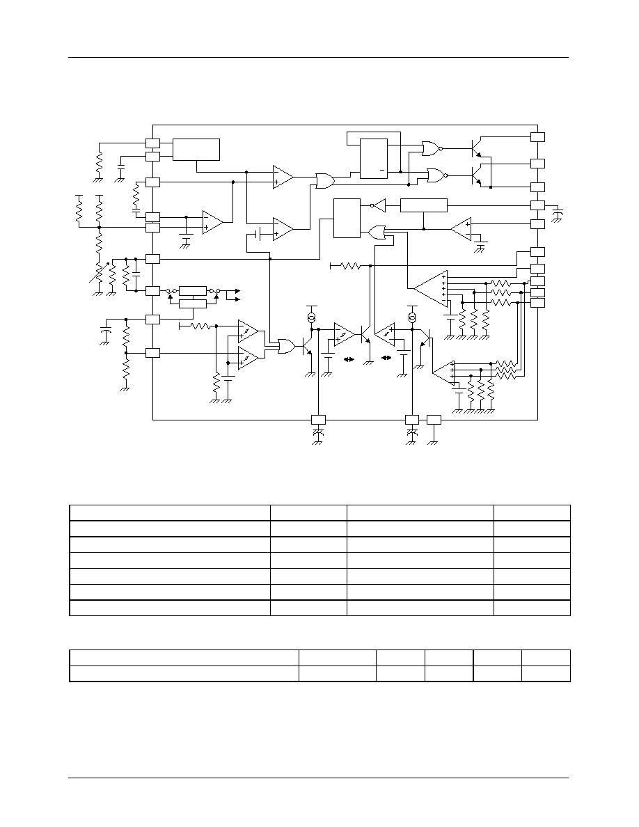
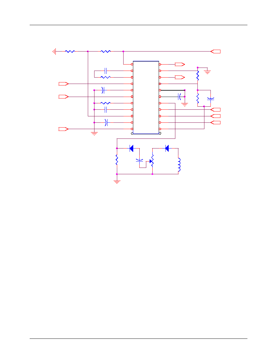
Internal Block Diagram
Absolute Maximum Ratings
Temperature Characteristics
Parameter
Symbol
Value
Unit
Supply voltage
V
CC
40
V
Collector output voltage
V
C1
, V
C2
40
V
Collector output current
I
C1
, I
C2
200
mA
Power dissipation(KA3511BS)
P
D
1.5
W
Operating temperature
T
OPR
-
25 to 85
°
C
Storage temperature
T
STG
-
65 to 150
°
C
Parameter
Symbol
Min.
Typ.
Max.
Unit
Temperature coefficient of Vref (-25
°
C
Ta
85
°
C)
Vref/
T
-
0.01
-
%/
°
C
7
8
OSCILLATOR
2
3
4
21
14
VREF
Start Up
1
9
DELAY
CONTROLLER
19
20
10
22
24
23
5
6
T
REM
11
18
15
16
17
PT
V12
V5
V3.3
PG
REM
(PS-ON)
E
C2
C1
REMOTE ON/OFF
1.4V
1.25
V
VREF
5V
OVP
COMP
1.25
V
UVP
COMP
GND
T
UVP
2.2uF
T
PG
2.2u
F
COMP3
1.8V
0.6V 1.8V
0.6V
PG
GENERATOR
VREF
Ichag
COMP2
COMP1
1.25V
0.1V
DEAD TIME
CONTROLLER
PWM
CONTROL
Q
R
S
CK
D
Q
Q
1.25V
INTERNAL
BIAS
5V
DET
V
CC
VREF
DEAD TIME
CONTROL
E/A(+
)
E/A(-
)
V5
V12
COMP
C
T
R
T
KA3511BS
3
Pin Definition : KA3511BS
Pin
Number
Pin
Name
I/O
Pin Function
Pin
Number
Pin
Name
I/O
Pin Function Descrition
1
V
CC
I
Supply voltage
13
NC
-
NC
2
COMP
O
E/A output
14
Vref
O
Precision reference VTG
3
E/A(-)
I
E/A (-) input
15
V3.3
I
OVP, UVP input for 3.3V
4
E/A(+)
I
E/A (+) input
16
V5
I
OVP, UVP input for 5V
5
TREM
-
Remote on/off delay
17
V12
I
OVP, UVP input for 12V
6
REM
I
Remote on/off input
18
PT
I
Extra protection input
7
RT
-
Oscillation freq. setting R
19
T
UVP
-
UVP delay
8
CT
-
Oscillation freq. setting C
20
GND
-
Signal ground
9
DET
I
Detect input
21
DTC
I
Deadtime control input
10
T
PG
-
PG delay
22
C2
O
Output 2
11
PG
O
Power good signal output
23
E
-
Power ground
12
NC
-
NC
24
C1
O
Output 1
KA3511D
#1
#12
#13
#24
Vcc
COMP
E/A(-)
EA(+)
TREM
REM
RT
CT
DET
TPG
PG
NC
C1
E
C2
DTC
GND
TUVP
PT
V12
V5
V3.3
Vref
NC
AS
BS

KA3511BS
4
Pin Number Pin Name
Pin Function Descrition
1
V
CC
Supply voltage. Operating range is 10V~30V. V
CC
=20V, Ta=25
°
C at test.
2
COMP
Error amplifier output. It is connected to non-inverting input of pulse width modulator
comparator.
3
E/A(-)
Error amplifier inverting input. Its reference voltage is always 1.25V.
4
E/A(+)
Error amplifier non-inverting input feedback voltage.This pin may be used to sense
power supply output voltage.
5
TREM
Remote on/off delay. Ton/Toff=8ms/24ms (Typ.) with C=0.1uF. Its high/low threshold
voltage is 1.8V/0.6V.
6
REM
Remote on/off input. It is TTL operation and its threshold voltage is 1.4V. Voltage at
this pin can reach normal 4.6V, with absolutely maximum voltage, 5.25V.
If REM =
"
Low
"
, PWM =
"
Low
"
. That means the main SMPS is operational.
When REM =
"
High
"
, then PWM =
"
High
"
and the main SMPS is turned-off.
7
RT
Oscillation frequency setting R. (Test Condition R
T
=10k
)
8
CT
Oscillation frequency setting C. (Test Condition C
T
=0.01uF)
9
DET
Under voltage detection pin. Its threshold voltage is 1.25V Typ.
10
T
PG
PG delay. Td=250ms (Typ) with C
PG
=2.2uF. The high/low threshold voltage are 1.8V/
0.6V and the voltage of Pin10 is clamped at 2.9V for noise margin.
11
PG
Power good output signal. PG =
"
High
"
means that the power is
"
Good
"
for operation
and PG =
"
Low
"
means
"
Power fail
"
.
14
Vref
Precision voltage reference trimmed to 2%. (Typical Value = 5.03V)
15
V3.3
OVP, UVP input for output 3.3V. (Typical Value = 4.1V/2.3V)
16
V5
OVP, UVP input for output 5V. (Typical Value = 6.2V/4.0V)
17
V12
OVP, UVP input for output 12V. (Typical Value = 14.2V/10V)
18
PT
This is prepared for an extra OVP input or another protection signal.
(Typical Value = 1.25V)
19
T
UVP
Timing pin for under voltage protection blank-out time. Its threshold voltage is 1.8V
and clamped at 2.9V after full charging. Target of delay time is 250ms and it is
realized through external (C=2.2uF).
20
GND
Signal ground.
21
DTC
Deadtime control input. The dead-time control comparator has an effective 120mV
input offset which limits the minimum output dead time. Dead time may be imposed
on the output by setting the dead time control input to a fixed voltage, ranging
between 0V to 3.3V.
22
C2
Output drive pin for push-pull operation.
23
E
Power ground.
24
C1
Output drive pin for push-pull operation.
KA3511BS
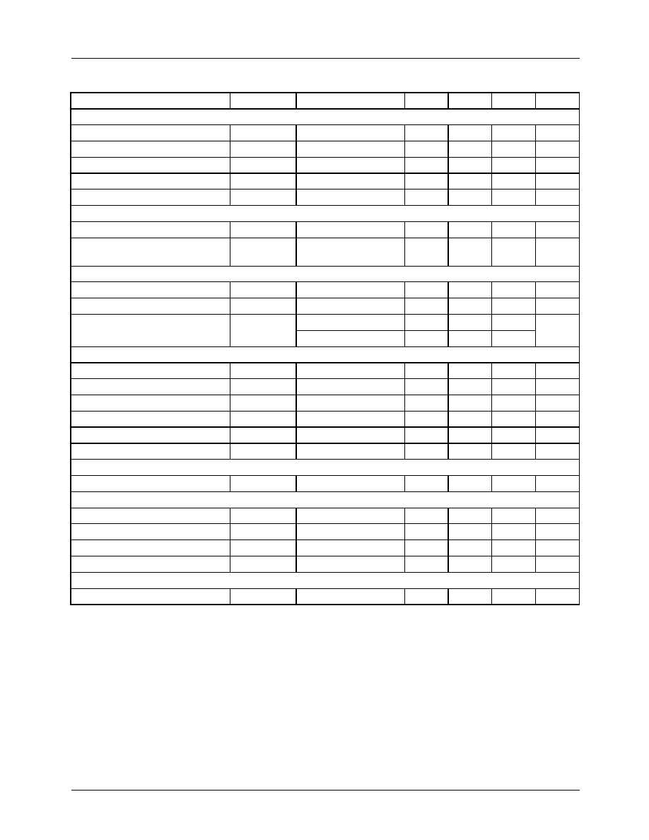
5
Electrical Characteristics (V
cc
=20V, T
a
=25
°
°
°
°
C)
Parameter
Symbol
Condition
Min.
Typ.
Max.
Unit
REFERENCE SECTION
Reference output voltage
Vref
Iref=1mA
4.9
5
5.1
V
Line regulation
Vref.
LINE
10V
V
CC
30V
-
2.0
25
mV
Load regulation
Vref.
LOAD
1mA
Iref
10mA
-
1.0
15
mV
Temperature coefficient of Vref
(1)
Vref/
T
-25
°
C
Ta
85
°
C
-
0.01
-
%/
°
C
Short-circuit output current
I
SC
Vref=0
15
35
75
mA
OSCILLATOR SECTION
Oscillation frequency
fosc
C
T
=0.01uF, R
T
=12k
-
10
-
kHz
Frequency change with
temperature
(1)
fosc/T
C
T
=0.01uF, R
T
=12k
-
2
-
%
DEAD TIME CONTROL SECTION
Input bias current
I
B(DT)
-
-
-2.0
-10
uA
Maximum duty voltage
DC
MAX
Pin19 (DTC)=0V
45
48
50
%
Input threshold voltage
V
TH(DT)
Zero Duty Cycle
-
3.0
3.3
V
Max. Duty Cycle
0
-
-
ERROR AMP SECTION
Inverting reference voltage
Vref(EA)
-
1.20
1.25
1.30
V
Input bias current
I
B(EA)
V
COMP
=2.5V
-
-0.1
-1.0
uA
Open-loop voltage gain
(1)
G
VO
0.5V
V
COMP
3.5V
70
95
-
dB
Unit-gain bandwidth
(1)
BW
-
-
650
-
kHz
Output sink current
I
SINK
V
COMP
=0.7V
0.3
0.9
-
mA
Output source current
I
SOURCE
V
COMP
=3.5V
-2.0
-4.0
-
mA
PWM COMPARATOR SECTION
Input threshold voltage
V
TH(PWM)
Zero Duty Cycle
-
4
4.5
V
OUTPUT SECTION
Output saturation voltage
V
CE(SAT)
I
C
=200mA
-
1.1
1.3
V
Collector off-state current
I
C(off)
V
CC
=V
C
=30V, V
E
=0V
-
2
100
uA
Rising time
T
R
-
-
100
200
ns
Falling time
T
F
-
-
50
200
ns
PROTECTION SECTION
Over voltage protection for 3.3V
V
OVP1
-
3.8
4.1
4.3
V
KA3511BS
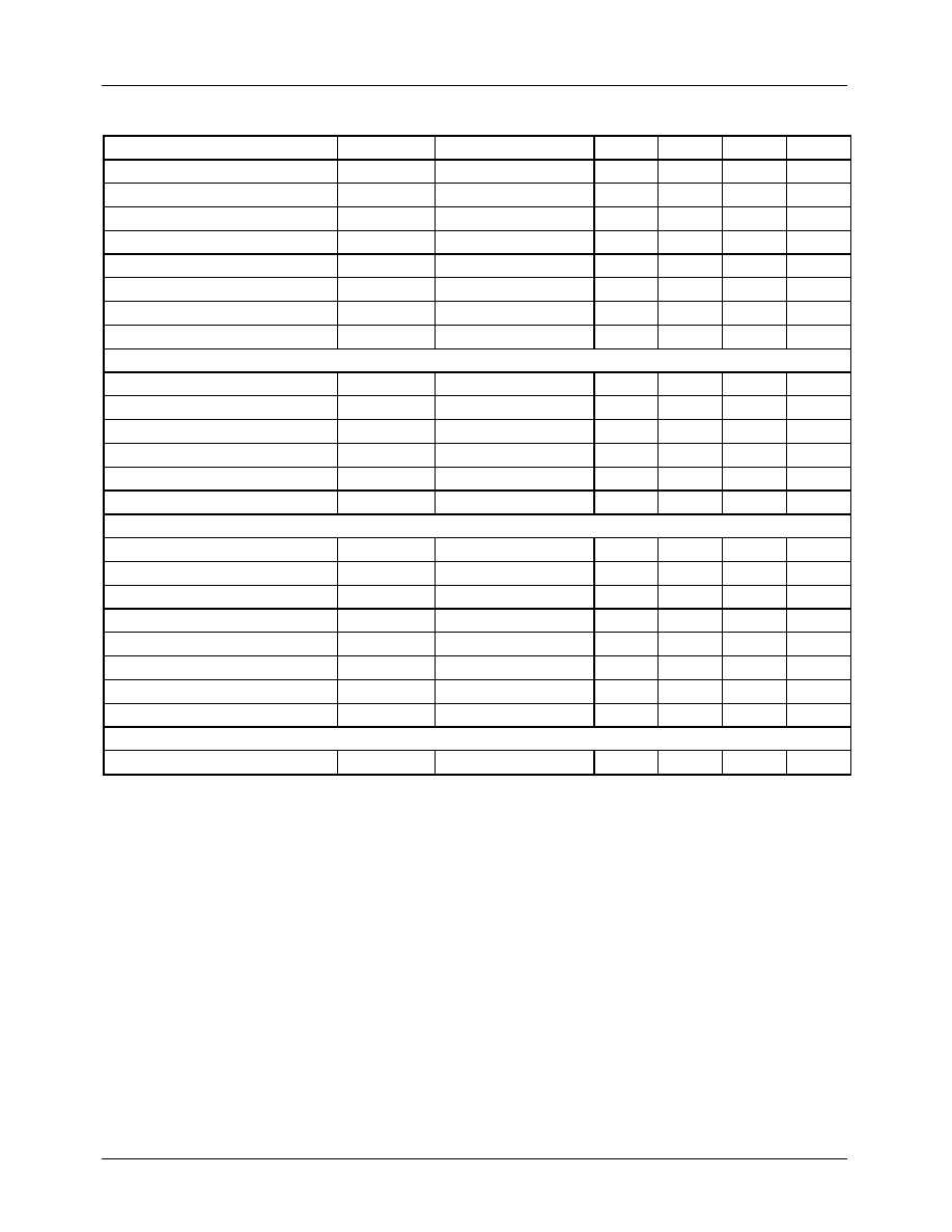
6
Electrical Characteristics (continued)
Note:
1. These Parameters, although guaranteed over their recommended operating conditions are not 100% tested in production.
2. REM on delay time (Pin6 REM:
"
L
"
"
H
"
),
REM off delay time (Pin6 REM:
"
H
"
"
L
"
)
Parameter
Symbol
Condition
Min.
Typ.
Max.
Unit
Over voltage protection for 5V
V
OVP2
-
5.8
6.2
6.6
V
Over voltage protection for 12V
V
OVP3
-
13.5
14.2
15.0
V
Input threshold voltage for PT
V
PT
-
1.20
1.25
1.30
V
Under voltage protection for 3.3V
V
UVP1
-
2.1
2.3
2.5
V
Under voltage protection for 5V
V
UVP2
-
3.7
4.0
4.3
V
Under voltage protection for 12V
V
UVP3
-
9.2
10
10.8
V
Charging current for UVP delay
I
CHG.UVP
C=2.2uF, V
TH
=1.8V
-
10
-
15
-
23
uA
UVP Delay Time
T
D.UVP
C=2.2uF
100
260
500
ms
REMOTE ON/OFF SECTION
REM on input voltage
V
REMH
I
REM
=
-
200uA
2.0
-
-
V
REM off input voltage
V
REML
-
-
-
0.8
V
REM off input bias voltage
I
REML
V
REM
=0.4V
-
-
-
1.6
mA
REM on open voltage
V
REM(OPEN)
-
2.0
-
5.25
V
REM on delay time
Ton
C=0.1uF
4
8
14
ms
REM off delay time
Toff
C=0.1uF
16
24
34
ms
REMOTE ON/OFF SECTION
(2)
Detecting input voltage
V
IN(DET)
-
1.20
1.25
1.30
V
Detecting V5 voltage
V5
(DET)
-
4.1
4.3
4.5
V
Hysteresis voltage 1
HY1
COMP1, 2
10
40
80
mV
Hysteresis voltage 2
HY2
COMP3
0.6
1.2
-
V
PG output load resistor
R
PG
-
0.5
1
2
k
Charging current for PG delay
I
CHG.PG
C=2.2uF, V
TH
=1.8V
-
10
-
15
-
23
uA
PG delay time
T
D.PG
C=2.2uF
100
260
500
ms
PG output saturation voltage
V
SAT(PG)
I
PG
=10mA
-
0.2
0.4
V
TOTAL DEVICE
Stanby supply current
I
CC
-
-
10
20
mA
KA3511BS
7
Application Informations
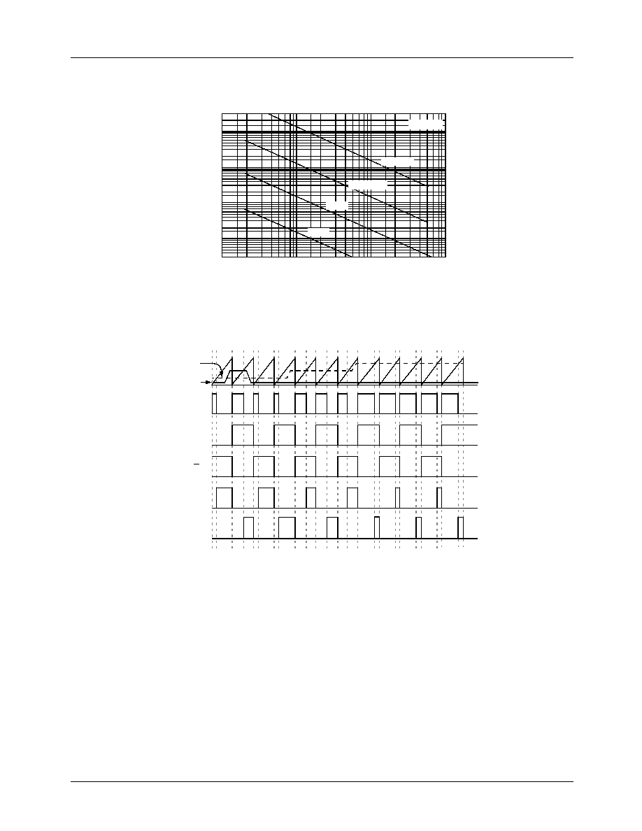
Figure 1. Oscillator Frequency vs. Timing Resistance
Figure 2. Operating Waveform
300K
2K
5K 10K
20K
50K 100K 200K
500K 1M
100K
10K
1K
100
30
1K
I
O
-
OSCI
LL
A
T
OR
FREQUENCY
R
T
. TIMING RESISTANCE(
)
VCC=15V
1.0
µ
F
0.1
µ
F
CT=0.01
µ
F
0.001
µ
F
Feedback
Dead-time
control
Ct
Ck
Q
Q
Output Q1
Output Q2
KA3511BS
8
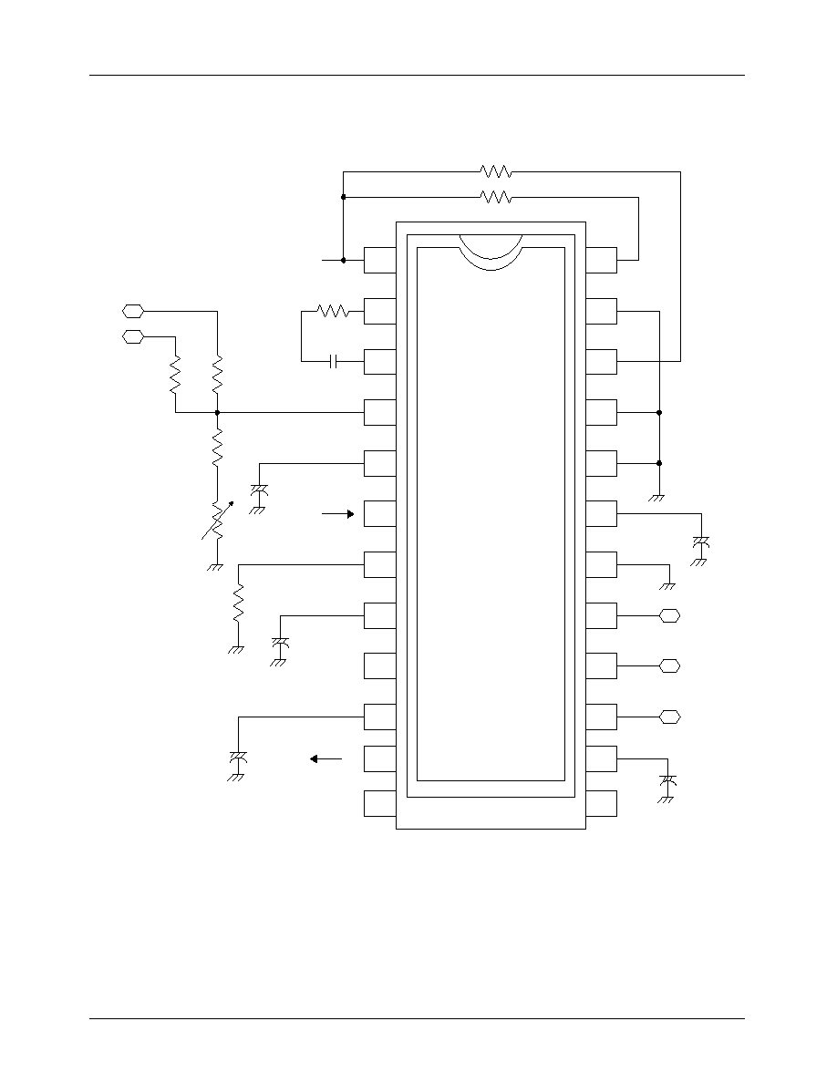
Housekeeping Circuit
Note :
The KA3511BS requires few external components to accomplish a complete housekeeping circuits for SMPS.
24
23
22
21
20
19
18
17
16
15
14
4
5
6
7
8
9
10
11
1
2
3
VCC
COMP
E/A(-)
E/A(+)
REM
RT
CT
DET
T
PG
PG
T
REM
C1
E
C2
DTC
GND
T
UVP
PT
V12
V5
V3.3
Vref
2k
(1W
)
15k
0.01u
F
12k
2.2uF
2k
(1W
)
11k
33k
1.8k
0.1uF
1k
0.01u
F
+
+
PG
Micom
12V
5V
Standby
Supply
V
CC
=20V
+
12V
5V
3V
K
K
K
K
A
A
A
A
3
3
3
3
5
5
5
5
1
1
1
1
1
1
1
1
A
A
A
A
2.2uF
+
1uF
+
12
13
S
B
KA3511BS
9
Typical Characteristics
0.014
0.012
0.010
0.008
0.006
0.004
0.002
0.000
0
10
20
30
40
Supply Voltage [V]
50
40
30
20
10
0
0.0
0.5
1.0
1.5
2.0
2.5
3.0
2.73
Deadtime Control Voltage [V]
7
6
5
4
3
2
1
0
5.0
5.5
6.0
6.5
7.0
I
CC
[A
]
Du
ty
Ra
ti
o
[%
]
31.1%
21.8%
12.8%
V5 [V]
5.010
5.008
5.006
5.004
5.002
-40
-20
0
20
40
60
80
100
120 140
TEMP [
°
C]
Vr
e
f
[
V
]
V
PG
[V
]
5
4
3
2
1
0
3.6
3.8
4.0
4.2
4.4
4.6
V3.3 [V]
V
PG
[V
]
5
4
3
2
1
0
14.0
14.2
14.4
14.6
14.8
15.0
V12 [V]
V
PG
[V
]
Figure 3.
V
CC
-I
CC
Figure 4.
Bandgap Reference Voltage
Figure 5.
PIN19(Dead Time Control Voltage)-Duty Cycle
Figure 6.
OVP for 3.3V
Figure 7.
OVP for 5V
Figure 8.
OVP for 12V
KA3511BS
10
Typical Characteristics
(Continued)
5
4
3
2
1
0
1.15
1.20
1.25
1.30
1.35
Vpt [V]
V
PG
[V
]
V
PG
[V
]
Pin 13 (V3.3) Voltage [V]
5
4
3
2
1
0
21
22
23
24
25
V
PG
[V
]
5
4
3
2
1
0
3.6
3.8
4.0
4.2
4.4
4.6
4.8
5.0
Pin 14 (V5) Voltage [V]
Pin 15 (V12) Voltage [V]
5
4
3
2
1
0
9.0
9.5
10.0
10.5
11.0
V
PG
[V
]
5
4
3
2
1
0
0
1
2
3
4
5
V
PG
[V
]
Vrem [V]
-0.000016
-0.000018
-0.000020
-0.000022
-0.000024
0
50
100
150
200
250
Ir
e
m
[A
]
Figure 9. OVP for PT
Figure 10. UVP for 3.3V
Figure 11 . UVP for 5V
Figure 12 . UVP for 12V
Figure 13 . Remote ON Charging Current
Figure 14 . REM ON/OFF Vth
KA3511BS
11
Typical Characteristics
(Continued)
5
4
3
2
1
0
0
1
2
3
4
5
Vrem
[
V
]
V
PG
[V
]
5
4
3
2
1
0
1.0
1.1
1.2
1.3
1.4
1.5
-0.000005
-0.000010
-0.000015
-0.000020
0
20
40
60
80 100 120 140 160
I
PG
[V
]
5
4
3
2
1
0
4.0
4.2
4.4
4.6
4.8
5.0
Pin 14 (5V) Voltage [V]
V
PG
[V
]
-0.032
-0.033
-0.034
-0.035
0
100
200
300
400
Ir
e
f
[A
]
5
4
3
2
1
0
0.0
0.5
1.0
1.5
2.0
2.5
V
PG
[V
]
Pin 9 (DET) Voltage [V]
Pin 10 (T
PG
) Voltage [V]
Figure 15. Remote ON Open Voltage
Figure 16. Detecting V
CC
Voltage (DET)
Figure 17. Detecting V5 Voltage
Figure 18. Charging Current for PG
Figure 19. Short Circuit Current
Figure 20. Hysteresis Voltage 2
KA3511BS
12
Typical Characteristics
(Continued)
0.002
0.00
-0.002
-0.004
-0.006
-0.008
0
20
40
60
80
100
120
140
I
s
i
n
k &
Iso
u
r
ce
[
A
]
5
4
3
2
1
0
0
10
20
30
40
V
r
e
f
[V
]
Supply Voltage [V]
Figure 21. Error Amp Sink Current
Figure 22. Reference Voltage
KA3511BS
13
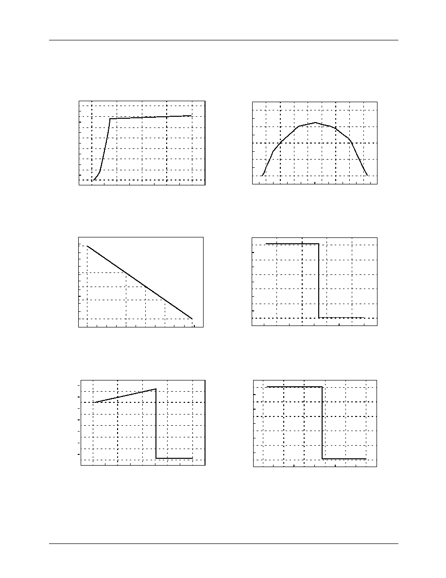
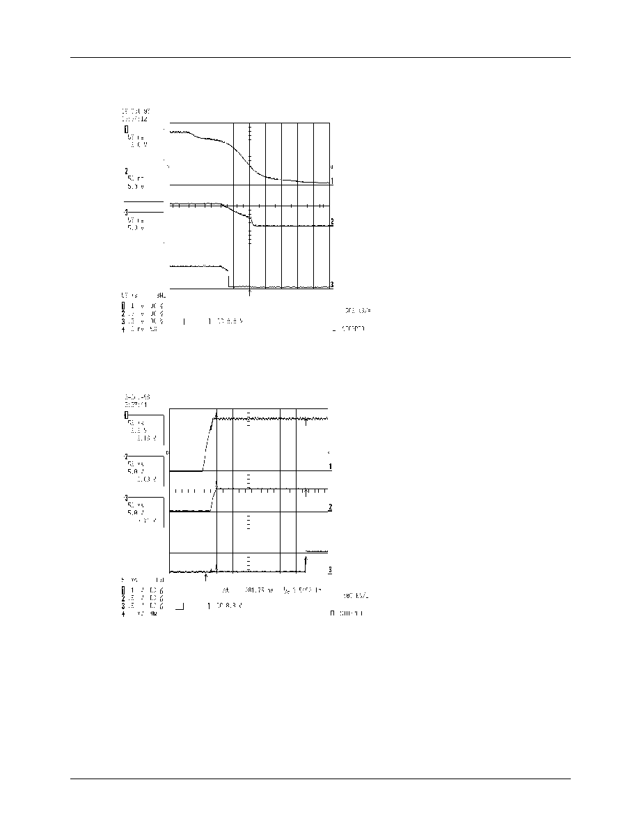
Experimental Result
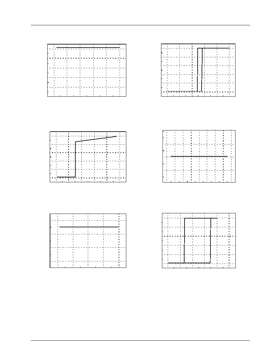
CH1 : PS-ON
CH2 : +5Vdc Output
CH3 : PG Signal
Figure 23. Rising Time of +5Vdc Output Voltage
Figure 24. PG Signal Delay Time
CH1 : PS-ON
CH2 : +5Vdc Output
CH3 : PG Signal
KA3511BS
14
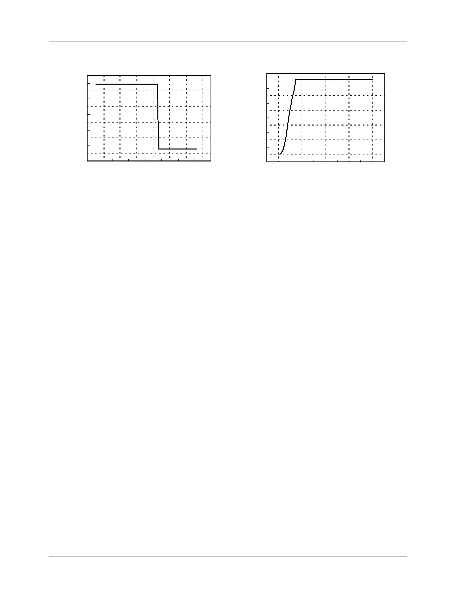
CH1 : PS-ON
CH2 : +5Vdc Output
CH3 : PG Signal
CH1 : +3.3Vdc Output
CH2 : +5Vdc Output
CH3 : +12Vdc Output
Figure 25. Power Down Warning
Figure 26. No Load Protection
KA3511BS
15
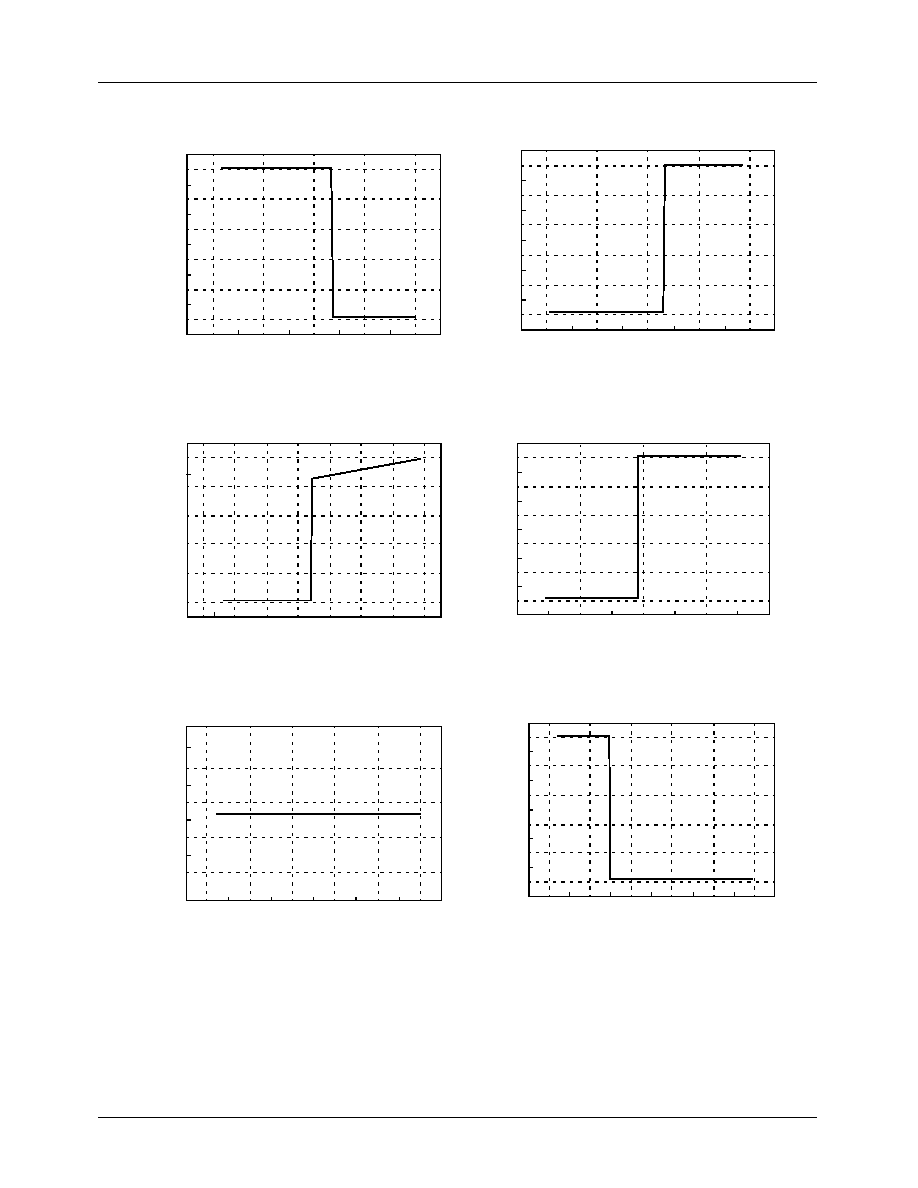
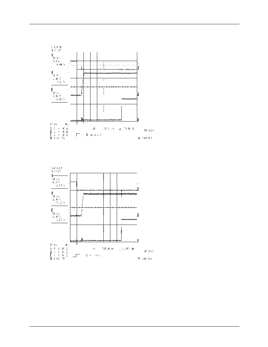
Figure 27. Vcc, +5Vdc Output vs. PG Signal (High)
Figure 28. Vcc, +5Vdc Output vs. PG Signal (Low)
CH1 : Vcc
CH2 : +5Vdc Output
CH3 : PG Signal
CH1 : Vcc
CH2 : +5Vdc Output
CH3 : PG Signal
KA3511BS
16
Application Circuit
C6
22uF
+
2.2uF
+
IC1
AR3511X
Vcc
1
C1
22
COMP
2
E
21
E/A(-)
3
C2
20
DTC
19
E/A(+)
4
TREM
5
GND
18
REM
6
TUVP
17
RT
7
PT
16
CT
8
V12
15
DET
9
V5
14
TPG
10
V3.3
13
PG
11
Vref
12
CT
15K
R5
70K
R6
47K
R4
1.2K
R3
56K
100K
103
0.1uF
+
C16
+
2.2uF
+
103
D19
D9
VR1
5V OUT
12V OUT
POWER ON
OUT REF
PG
3.3V OUT
VCC
C1
C2
24
23
22
21
20
19
18
17
16
15
14
B
13
12
NC
NC
S
NC
NC
KA3511BS
KA3511BS
17
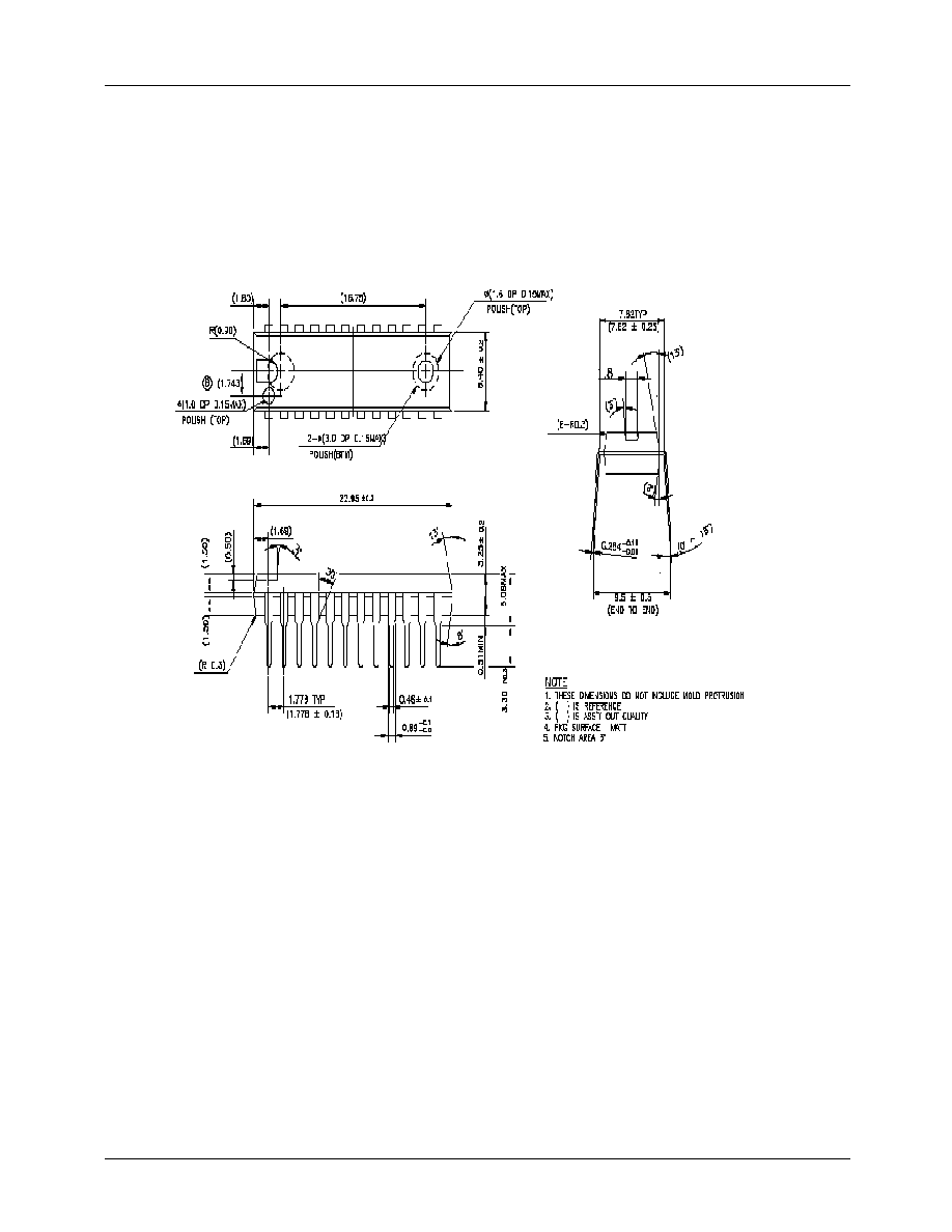
Mechanical Dimensions
Package
Dimensions in millimeters
24-SDIP

KA3511BS
18
Ordering Information
Product Number
Package
Operating Temperature
KA3511BS
24-SDIP
0
°
C ~ 70
°
C

KA3511BS
19

KA3511BS
7/2/01 0.0m 001
Stock#DSxxxxxxxx
2001 Fairchild Semiconductor Corporation
LIFE SUPPORT POLICY
FAIRCHILD'S PRODUCTS ARE NOT AUTHORIZED FOR USE AS CRITICAL COMPONENTS IN LIFE SUPPORT DEVICES
OR SYSTEMS WITHOUT THE EXPRESS WRITTEN APPROVAL OF THE PRESIDENT OF FAIRCHILD SEMICONDUCTOR
CORPORATION. As used herein:
1. Life support devices or systems are devices or systems
which, (a) are intended for surgical implant into the body,
or (b) support or sustain life, and (c) whose failure to
perform when properly used in accordance with
instructions for use provided in the labeling, can be
reasonably expected to result in a significant injury of the
user.
2. A critical component in any component of a life support
device or system whose failure to perform can be
reasonably expected to cause the failure of the life support
device or system, or to affect its safety or effectiveness.
www.fairchildsemi.com
DISCLAIMER
FAIRCHILD SEMICONDUCTOR RESERVES THE RIGHT TO MAKE CHANGES WITHOUT FURTHER NOTICE TO ANY
PRODUCTS HEREIN TO IMPROVE RELIABILITY, FUNCTION OR DESIGN. FAIRCHILD DOES NOT ASSUME ANY
LIABILITY ARISING OUT OF THE APPLICATION OR USE OF ANY PRODUCT OR CIRCUIT DESCRIBED HEREIN; NEITHER
DOES IT CONVEY ANY LICENSE UNDER ITS PATENT RIGHTS, NOR THE RIGHTS OF OTHERS.