 | –≠–ª–µ–∫—Ç—Ä–æ–Ω–Ω—ã–π –∫–æ–º–ø–æ–Ω–µ–Ω—Ç: KA358S | –°–∫–∞—á–∞—Ç—å:  PDF PDF  ZIP ZIP |
©2002 Fairchild Semiconductor Corporation
www.fairchildsemi.com
Rev. 1.0.2
Features
∑ Internally Frequency Compensated for Unity Gain
∑ Large DC Voltage Gain: 100dB
∑ Wide Power Supply Range:
KA258/KA258A, KA358/KA358A: 3V ~ 32V (or
±1.5V~ 16V)
KA2904 : 3V~26V (or ±1.5V ~ 13V)
∑ Input Common Mode Voltage Range Includes Ground
∑ Large Output Voltage Swing: 0V DC to Vcc - 1.5V DC
∑ Power Drain Suitable for Battery Operation.
Description
The KA258 series consist of two independent, high gain,
internally frequency compensated operational amplifiers
which were designed specifically to operate from a single
power supply over a wide range of voltage. Operation from
split power supplies is also possible and the low power
supply current drain is independent of the magnitude of the
power supply voltage. Application areas include transducer
amplifier, DC gain blocks and all the conventional OP-AMP
circuits which now can be easily implemented in single
power supply systems.
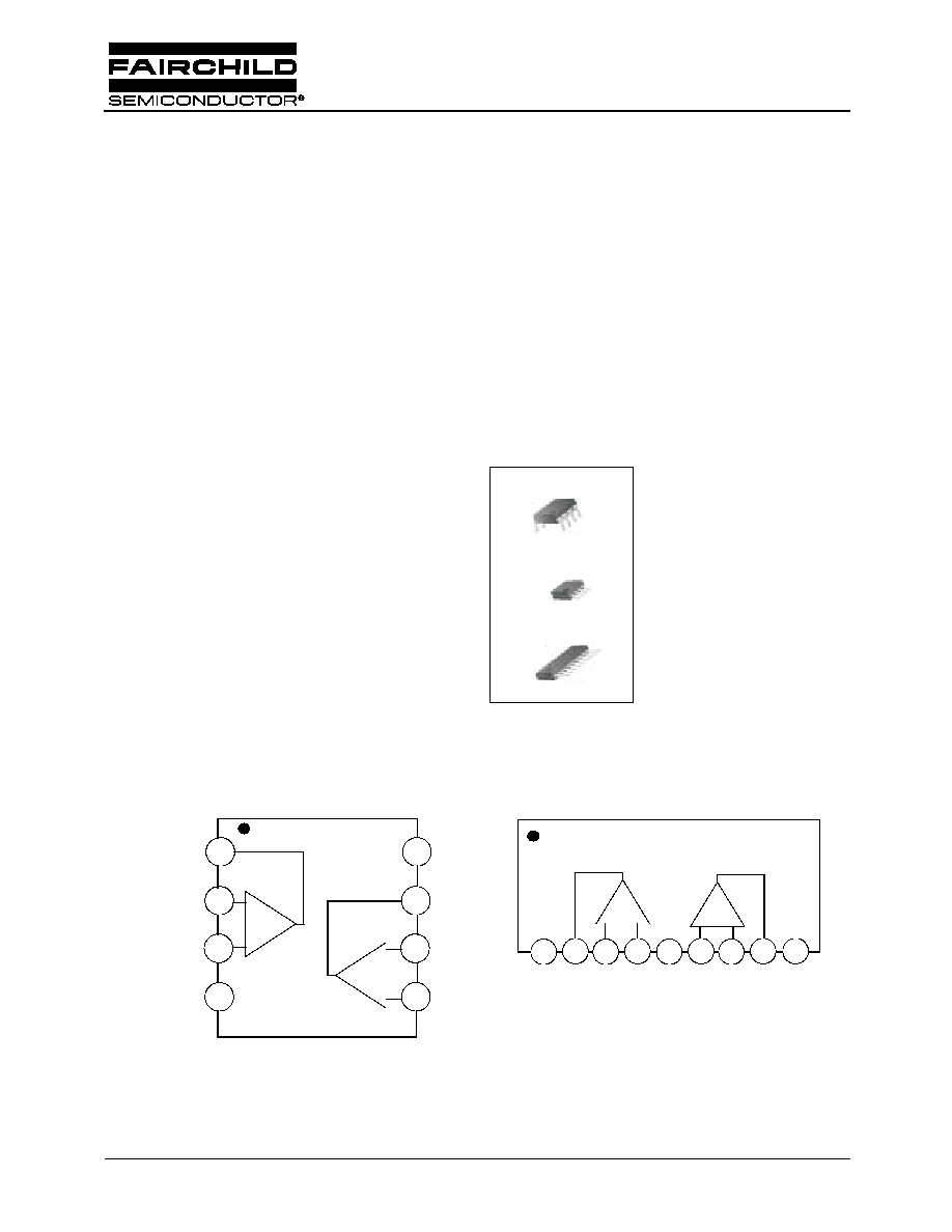
8-DIP
8-SOP
9-SIP
1
1
1
Internal Block Diagram
-
+
+
-
1
2
3
4
5
6
7
8 V
CC
OUT2
IN2 (-)
IN2 (+)
OUT1
IN1 (-)
IN1 (+)
GND
1
2
3
4
5
6
7
8
9
-
+
+
-
V
CC
OUT
1
I
N
1
(-)
IN
1(
+)
GN
D
IN
2(
+)
I
N
2
(-)
OUT
2
V
CC
KA258/KA258A, KA358/KA358A,
KA2904
Dual Operational Amplifier
KA258/KA258A, KA358/KA358A, KA2904
2
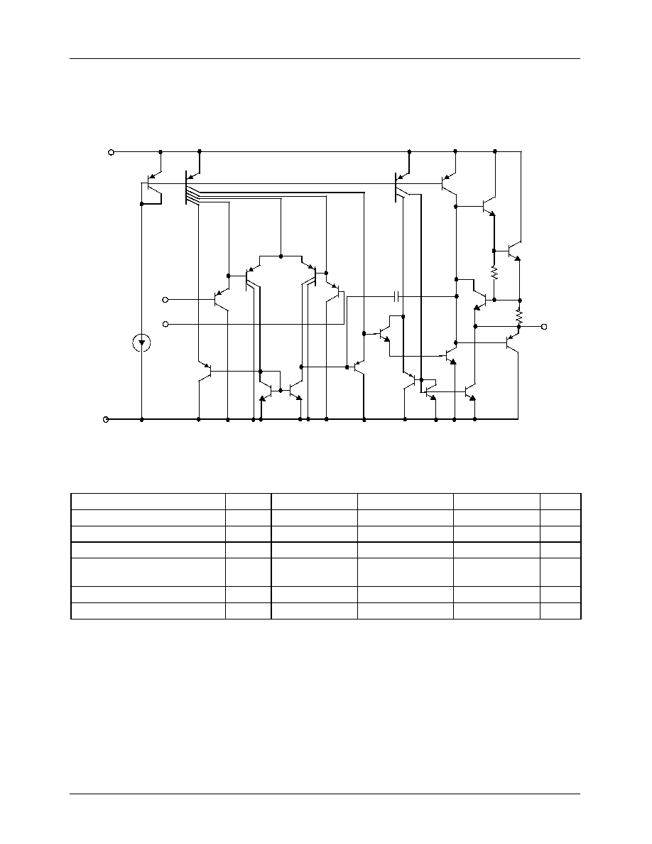
Schematic Diagram
(One section only)
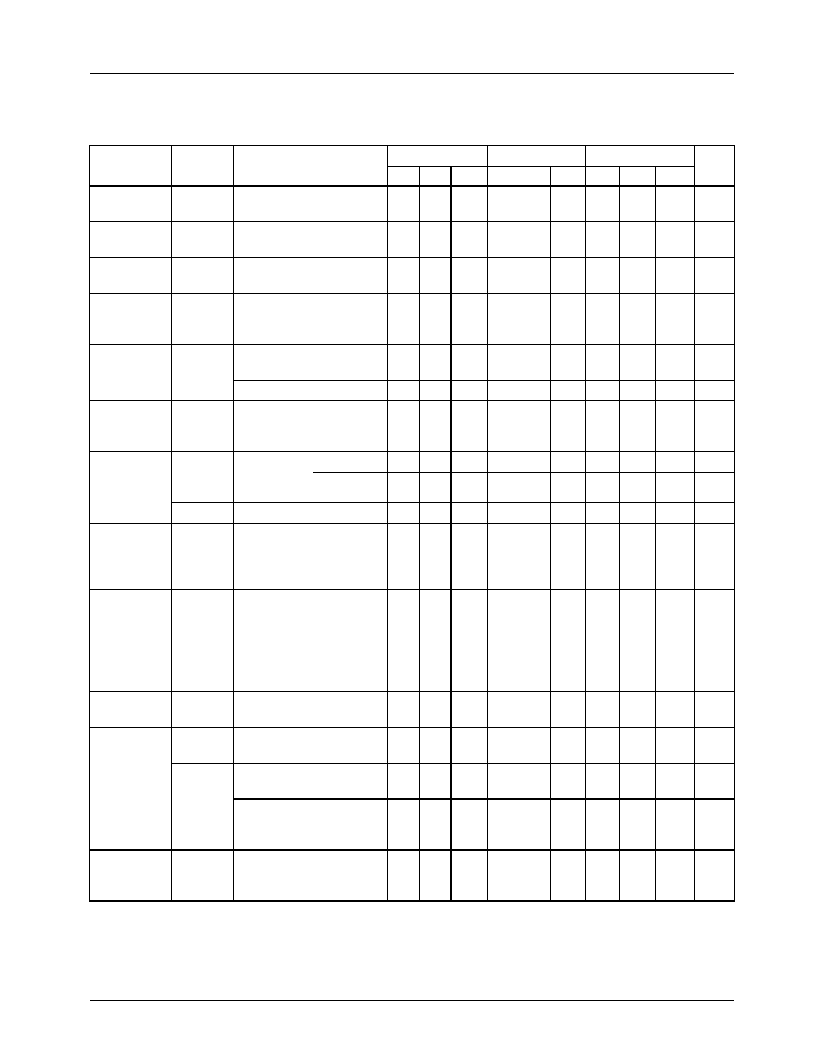
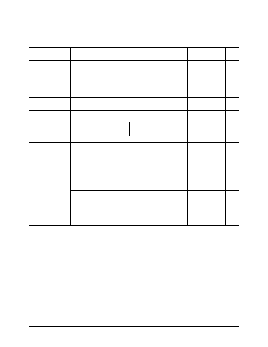
Absolute Maximum Ratings
Parameter
Symbol KA258/KA258A
KA358/KA358A
KA2904
Unit
Supply Voltage
V
CC
±
16 or 32
±
16 or 32
±
13 or 26
V
Differential Input Voltage
V
I(DIFF)
32
32
26
V
Input Voltage
V
I
-0.3 to +32
-0.3 to +32
-0.3 to +26
V
Output Short Circuit to GND
V
CC
15V, T
A
= 25
∞
C(One Amp)
-
Continuous
Continuous
Continuous
-
Operating Temperature Range
T
OPR
-25 ~ +85
0 ~ +70
-40 ~ +85
∞
C
Storage Temperature Range
T
STG
-65 ~ +150
-65 ~ +150
-65 ~ +150
∞
C
Q8
Q7
Q6
Q5
Q4
Q3
Q2
Q1
Q9
Q10
Q11
Q12
Q14
Q15
Q16
Q18
Q19
Q20
R2
Q21
C1
R1
GND
OUTPUT
IN(+)
IN(-)
V
CC
Q13
Q17
KA258/KA258A, KA358/KA358A, KA2904
3
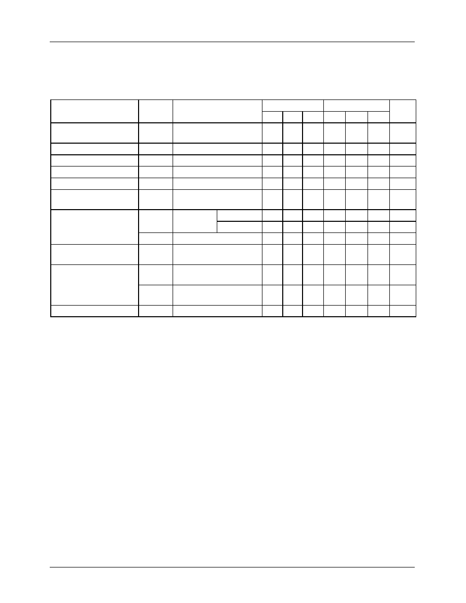
Electrical Characteristics
(Vcc = 5.0V, V
EE
= GND, T
A
= 25
∞
C, unless otherwise specified)
Note:
1. This parameter, although guaranteed, is not 100% tested in production.
Parameter Symbol
Conditions
KA258
KA358
KA2904
Unit
Min. Typ. Max. Min. Typ. Max. Min. Typ. Max.
Input Offset
Voltage
V
IO
V
CM
= 0V to V
CC
-1.5V
V
O(P)
= 1.4V, R
S
= 0
-
2.9
5.0
-
2.9
7.0
-
2.9
7.0
mV
Input Offset
Current
I
IO
-
-
3
30
-
5
50
-
5
50
nA
Input Bias
Current
I
BIAS
-
-
45
150
-
45
250
-
45
250
nA
Input
Voltage
Range
V
I(R)
V
CC
= 30V
(KA2904, V
CC
= 26V)
0
-
Vcc
-1.5
0
-
Vcc
-1.5
0
-
Vcc
-1.5
V
Supply
Current
I
CC
R
L
=
, V
CC
= 30V
(KA2904, V
CC
= 26V)
-
0.8
2.0
-
0.8
2.0
-
0.8
2.0
mA
R
L
=
, V
CC
= 5V
-
0.5
1.2
-
0.5
1.2
-
0.5
1.2
mA
Large Signal
Voltage
Gain
G
V
V
CC
= 15V, R
L
=
2k
V
O(P)
= 1V to 11V
50
100
-
25 100
-
25
100
-
V/mV
Output
Voltage
Swing
V
O(H)
V
CC
= 30V
(V
CC
= 26V
for KA2904)
R
L
= 2k
26
-
-
26
-
-
22
-
-
V
R
L
= 10k
27
28
-
27
28
-
23
24
-
V
V
O(L)
V
CC
= 5V, R
L
=
10k
-
5
20
-
5
20
-
5
20
mV
Common-
Mode
Rejection
Ratio
CMRR
-
70
85
-
65
80
-
50
80
-
dB
Power
Supply
Rejection
Ratio
PSRR
-
65
100
-
65 100
-
50
100
-
dB
Channel
Separation
CS
f = 1kHz to 20kHz
(Note1)
-
120
-
-
120
-
-
120
-
dB
Short Circuit
to GND
I
SC
-
-
40
60
-
40
60
-
40
60
mA
Output
Current
I
SOURCE
V
I(+)
= 1V, V
I(-)
= 0V
V
CC
= 15V, V
O(P)
= 2V
20
30
-
20
30
-
20
30
-
mA
I
SINK
V
I(+)
= 0V, V
I(-)
= 1V
V
CC
= 15V, V
O(P)
= 2V
10
15
-
10
15
-
10
15
-
mA
V
I(+)
= 0V, V
I(-)
= 1V
V
CC
= 15V,
V
O(P)
= 200mV
12
100
-
12 100
-
-
-
-
µ
A
Differential
Input
Voltage
V
I(DIFF)
-
-
-
V
CC
-
-
V
CC
-
-
V
CC
V
KA258/KA258A, KA358/KA358A, KA2904
4
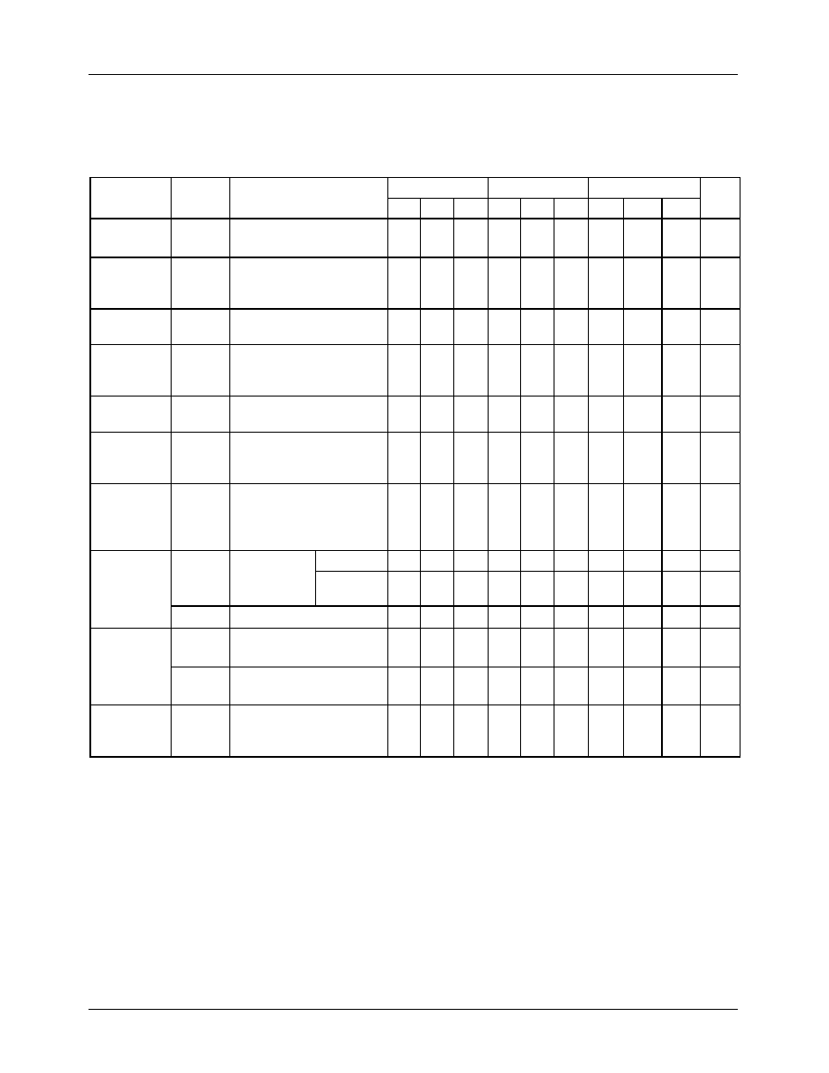
Electrical Characteristics
(Continued)
(V
CC
= 5.0V, V
EE
= GND, unless otherwise specified)
The following specification apply over the range of -25
∞
C
T
A
+85
∞
C for the KA258; and the 0
∞
C
T
A
+70
∞
C
for the KA358; and the -40
∞
C
T
A
+85
∞
C for the KA2904
Parameter
Symbol
Conditions
KA258
KA358
KA2904
Unit
Min. Typ. Max. Min. Typ. Max. Min. Typ. Max.
Input Offset
Voltage
V
IO
V
CM
= 0V to V
CC
-1.5V
V
O(P)
= 1.4V, R
S
= 0
-
-
7.0
-
-
9.0
-
-
10.0
mV
Input Offset
Voltage
Drift
V
IO/
T
R
S
= 0
-
7.0
-
-
7.0
-
-
7.0
-
µ
V/
∞
C
Input Offset
Current
I
IO
-
-
-
100
-
-
150
-
45
200
nA
Input Offset
Current
Drift
I
IO
/
T
-
-
10
-
-
10
-
-
10
-
pA/
∞
C
Input Bias
Current
I
BIAS
-
-
40
300
-
40
500
-
40
500
nA
Input
Voltage
Range
V
I(R)
V
CC
= 30V
(KA2904,V
CC
= 26V)
0
-
Vcc
-2.0
0
-
Vcc
-2.0
0
-
Vcc
-2.0
V
Large
Signal
Voltage
Gain
G
V
V
CC
= 15V, R
L
=
2.0k
V
O(P)
= 1V to 11V
25
-
-
15
-
-
15
-
-
V/mV
Output
Voltage
Swing
V
O(H)
V
CC
= 30V
(V
CC
= 26V
for KA2904)
R
L
= 2k
26
-
-
26
-
-
22
-
-
V
R
L
= 10k
27
28
-
27
28
-
23
24
-
V
V
O(L)
V
CC
= 5V, R
L
=
10k
-
5
20
-
5
20
-
5
20
mV
Output
Current
I
SOURCE
V
I(+)
= 1V, V
I(-)
= 0V
V
CC
= 15V, V
O(P)
= 2V
10
30
-
10
30
-
10
30
-
mA
I
SINK
V
I(+)
= 0V, V
I(-)
= 1V
V
CC
= 15V, V
O(P)
= 2V
5
8
-
5
9
-
5
9
-
mA
Differential
Input
Voltage
V
I(DIFF)
-
-
-
V
CC
-
-
V
CC
-
-
V
CC
V
KA258/KA258A, KA358/KA358A, KA2904
5
Electrical Characteristics
(Continued)
(V
CC
= 5.0V, V
EE
= GND, T
A
= 25
∞
C, unless otherwise specified)
Note:
1. This parameter, although guaranteed, is not 100% tested in production.
Parameter Symbol
Conditions
KA258A
KA358A
Unit
Min. Typ. Max. MIn. Typ. Max.
Input Offset Voltage
V
IO
V
CM
= 0V to V
CC
-1.5V
V
O(P)
= 1.4V, R
S
= 0
-
1.0
3.0
-
2.0
3.0
mV
Input Offset Current
I
IO
-
-
2
15
-
5
30
nA
Input Bias Current
I
BIAS
-
-
40
80
-
45
100
nA
Input Voltage Range
V
I(R)
V
CC
= 30V
0
-
V
CC
-1.5
0
-
V
CC
-1.5
V
Supply Current
I
CC
R
L
=
,V
CC
= 30V
-
0.8
2.0
-
0.8
2.0
mA
RL =
, V
CC
= 5V
-
0.5
1.2
-
0.5
1.2
mA
Large Signal
Voltage Gain
G
V
V
CC
= 15V, R
L
=
2k
V
O
= 1V to 11V
50
100
-
25
100
-
V/mV
Output Voltage
Swing
V
OH
V
CC
= 30V
R
L
= 2k
26
-
-
26
-
-
V
R
L
= 10k
27
28
-
27
28
-
V
V
O(L)
V
CC
= 5V, R
L
=
10k
-
5
20
-
5
20
mV
Common-Mode
Rejection Ratio
CMRR
-
70
85
-
65
85
-
dB
Power Supply
Rejection Ratio
PSRR
-
65
100
-
65
100
-
dB
Channel Separation
CS
f = 1kHz to 20kHz (Note1)
-
120
-
-
120
-
dB
Short Circuit to GND
I
SC
-
-
40
60
-
40
60
mA
Output Current
I
SOURCE
V
I(+)
= 1V, V
I(-)
= 0V
V
CC
= 15V, V
O(P)
= 2V
20
30
-
20
30
-
mA
I
SINK
V
I(+)
= 1V, V
I(-)
= 0V
V
CC
= 15V, V
O(P)
= 2V
10
15
-
10
15
-
mA
V
in(+)
= 0V, V
in (-)
= 1V
V
O(P)
= 200mV
12
100
-
12
100
-
µ
A
Differential Input
Voltage
V
I(DIFF)
-
-
-
V
CC
-
-
V
CC
V
KA258/KA258A, KA358/KA358A, KA2904
6
Electrical Characteristics
(Continued)
(V
CC
= 5.0V, V
EE
= GND, unless otherwise specified)
The following specification apply over the range of -25
∞
C
T
A
+85
∞
C for the KA258A; and the 0
∞
C
T
A
+70
∞
C
for the KA358A
Parameter Symbol
Conditions
KA258A
KA358A
Unit
Min. Typ. Max. Min. Typ. Max.
Input Offset Voltage
V
IO
V
CM
= 0V to V
CC
-1.5V
V
O(P)
= 1.4V, R
S
= 0
-
-
4.0
-
-
5.0
mV
Input Offset Voltage Drift
V
IO
/
T
-
-
7.0
15
-
7.0
20
µ
V/
∞
C
Input Offset Current
I
IO
-
-
-
30
-
-
75
nA
Input Offset Current Drift
I
IO
/
T
-
-
10
200
-
10
300
pA/
∞
C
Input Bias Current
I
BIAS
-
-
40
100
-
40
200
nA
Input Common-Mode
Voltage Range
V
I(R)
V
CC
= 30V
0
-
Vcc
-2.0
0
-
Vcc
-2.0
V
Output Voltage Swing
V
O(H)
V
CC
= 30V
R
L
= 2k
26
-
-
26
-
-
V
R
L
= 10k
27
28
-
27
28
-
V
V
O(L)
V
CC
= 5V, R
L
=
10k
-
5
20
-
5
20
mV
Large Signal Voltage
Gain
G
V
V
CC
= 15V, R
L
=
2.0k
V
O(P)
= 1V to 11V
25
-
-
15
-
-
V/mV
Output Current
I
SOURCE
V
I(+)
= 1V, V
I(-)
= 0V
V
CC
= 15V, V
O(P)
= 2V
10
30
-
10
30
-
mA
I
SINK
V
I(+)
= 1V, V
I(-)
= 0V
V
CC
= 15V, V
O(P)
= 2V
5
9
-
5
9
-
mA
Differential Input Voltage
V
I(DIFF)
-
-
-
V
CC
-
-
V
CC
V
KA258/KA258A, KA358/KA358A, KA2904
7
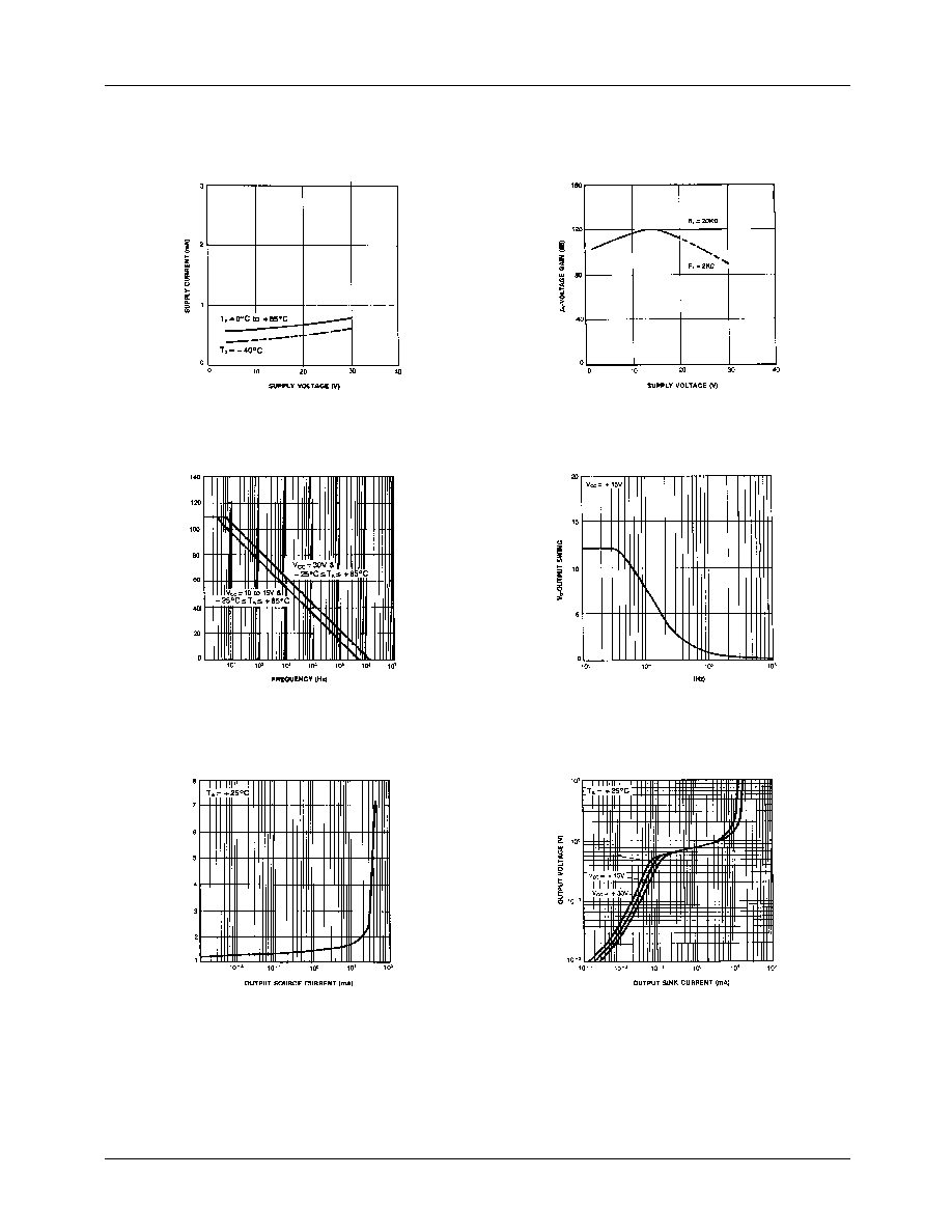
Typical Performance Characteristics
Figure 1. Supply Current vs Supply Voltage
Figure 2. Voltage Gain vs Supply Voltage
Figure 3. Open Loop Frequency Response
Figure 4. Large Signal Output Swing vs Frequency
Figure 5. Output Characteristics vs Current Sourcing
Figure 6. Output Characteristics vs Current Sinking
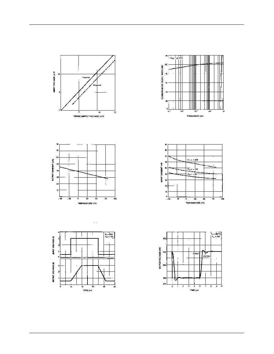
KA258/KA258A, KA358/KA358A, KA2904
8
Typical Performance Characteristics
(Continued)
Figure 7. Input Voltage Range vs Supply Voltage
Figure 8. Common-Mode Rejection Ratio
Figure 9. Output Current vs Temperature (Current Limiting)
Figure 10. Input Current vs Temperature
Figure 11. Voltage Follower Pulse Response
Figure 12. Voltage Follower Pulse Response
(Small Signal)
KA258/KA258A, KA358/KA358A, KA2904
9
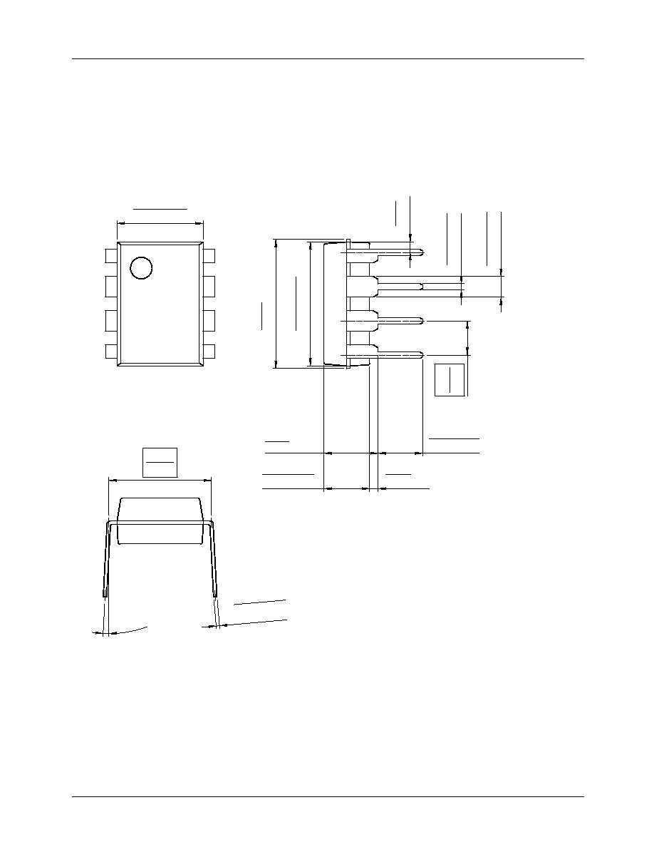
Mechanical Dimensions
Package
Dimensions in millimeters
6.40
±
0.20
3.30
±
0.30
0.130
±
0.012
3.40
±
0.20
0.134
±
0.008
#1
#4
#5
#8
0.252
±
0.008
9.20
±
0.20
0.79
2.54
0.100
0.031
()
0.46
±
0.10
0.018
±
0.004
0.060
±
0.004
1.524
±
0.10
0.362
±
0.008
9.60
0.378
MAX
5.08
0.200
0.33
0.013
7.62
0~15
∞
0.300
MAX
MIN
0.25
+0.10
≠0.05
0.010
+0.004
≠0.002
8-DIP
KA258/KA258A, KA358/KA358A, KA2904
10
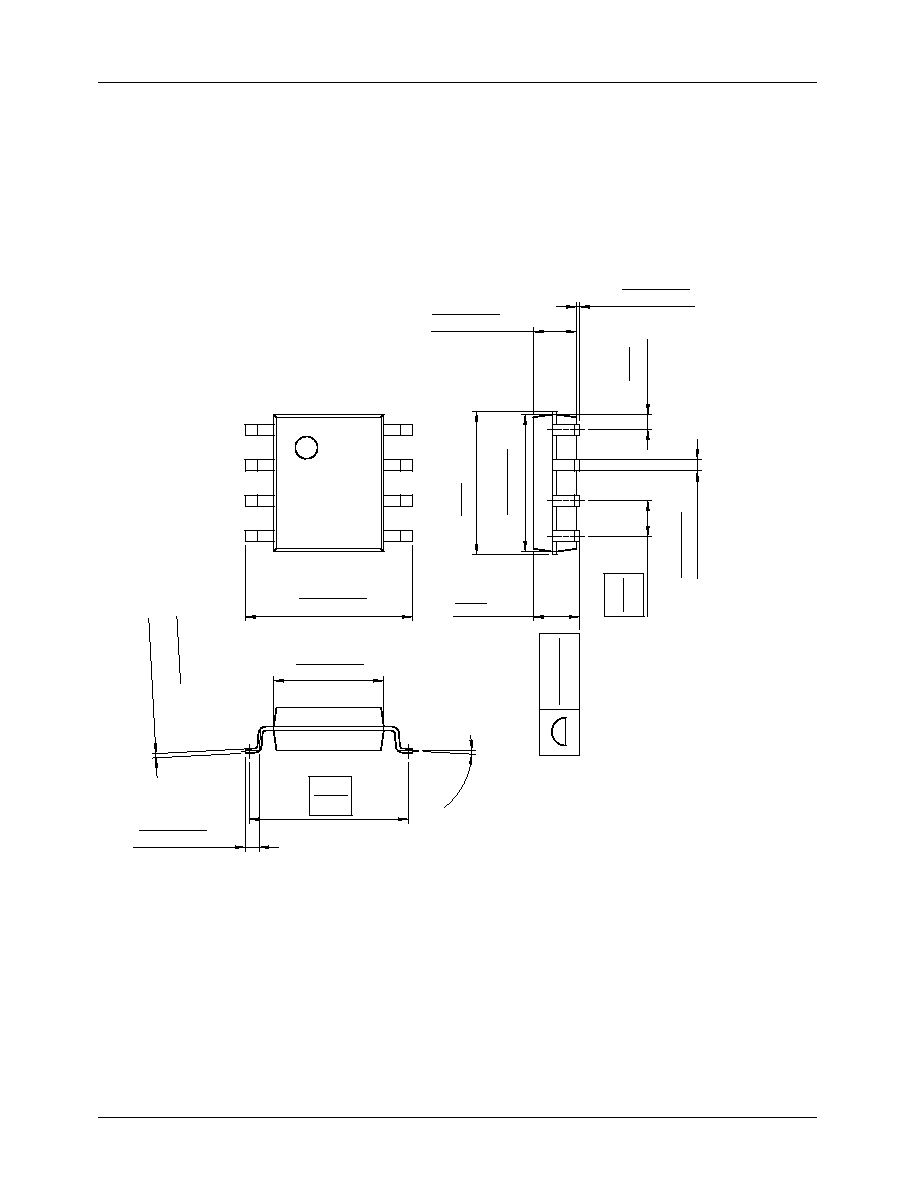
Mechanical Dimensions
(Continued)
Package
Dimensions in millimeters
4.92
±
0.20
0.194
±
0.008
0.41
±
0.10
0.016
±
0.004
1.27
0.050
5.72
0.225
1.55
±
0.20
0.061
±
0.008
0.1~0.25
0.004~0.001
6.00
±
0.30
0.236
±
0.012
3.95
±
0.20
0.156
±
0.008
0.50
±
0.20
0.020
±
0.008
5.13
0.202
MAX
#1
#4
#5
0~8
∞
#8
0.56
0.022
()
1.80
0.071
MAX0.10
MAX0.004
MAX
MIN
+
0.10
-0.05
0.15
+
0.004
-0.002
0.006
8-SOP
KA258/KA258A, KA358/KA358A, KA2904
11
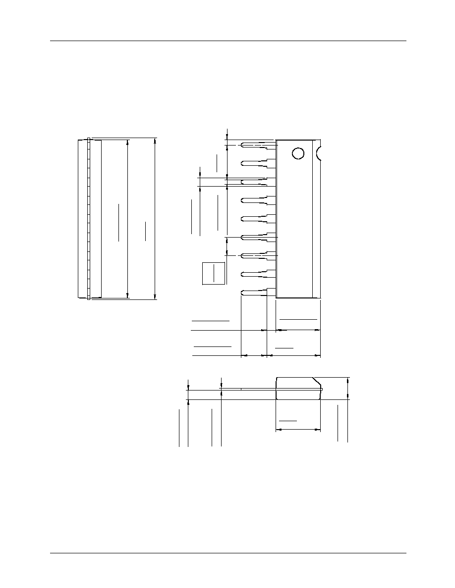
Mechanical Dimensions
(Continued)
Package
Dimensions in millimeters
21.84
±
0.20
0.860
±
0.008
22.24
0.876
MAX
1.20
±
0.10
0.047
±
0.004
0.60
±
0.10
0.024
±
0.004
0.76
0.030
()
2.54
0.100
1.15
±
0.20
0.045
±
0.008
5.80
±
0.20
0.228
±
0.008
3.30
±
0.30
0.130
±
0.012
7.30
0.287
MAX
#1
#9
1.25
±
0.10
3.00
±
0.20
0.118
±
0.008
0.049
±
0.004
0.25
±
0.10
0.010
±
0.004
6.00
0.236
MAX
9-SIP
KA258/KA258A, KA358/KA358A, KA2904
8/26/02 0.0m 001
Stock#DSxxxxxxxx
2002 Fairchild Semiconductor Corporation
LIFE SUPPORT POLICY
FAIRCHILD'S PRODUCTS ARE NOT AUTHORIZED FOR USE AS CRITICAL COMPONENTS IN LIFE SUPPORT DEVICES
OR SYSTEMS WITHOUT THE EXPRESS WRITTEN APPROVAL OF THE PRESIDENT OF FAIRCHILD SEMICONDUCTOR
CORPORATION. As used herein:
1. Life support devices or systems are devices or systems
which, (a) are intended for surgical implant into the body,
or (b) support or sustain life, and (c) whose failure to
perform when properly used in accordance with
instructions for use provided in the labeling, can be
reasonably expected to result in a significant injury of the
user.
2. A critical component in any component of a life support
device or system whose failure to perform can be
reasonably expected to cause the failure of the life support
device or system, or to affect its safety or effectiveness.
www.fairchildsemi.com
DISCLAIMER
FAIRCHILD SEMICONDUCTOR RESERVES THE RIGHT TO MAKE CHANGES WITHOUT FURTHER NOTICE TO ANY
PRODUCTS HEREIN TO IMPROVE RELIABILITY, FUNCTION OR DESIGN. FAIRCHILD DOES NOT ASSUME ANY
LIABILITY ARISING OUT OF THE APPLICATION OR USE OF ANY PRODUCT OR CIRCUIT DESCRIBED HEREIN; NEITHER
DOES IT CONVEY ANY LICENSE UNDER ITS PATENT RIGHTS, NOR THE RIGHTS OF OTHERS.
Ordering Information
Product Number
Package
Operating Temperature
KA358
8-DIP
0 ~ +70
∞
C
KA358A
KA358D
8-SOP
KA358AD
KA358S
9-SIP
KA358AS
KA258
8-DIP
-25 ~ +85
∞
C
KA258A
KA258D
8-SOP
KA258AD
KA2904
8-DIP
-40 ~ +85
∞
C
KA2904D
8-SOP