 | –≠–ª–µ–∫—Ç—Ä–æ–Ω–Ω—ã–π –∫–æ–º–ø–æ–Ω–µ–Ω—Ç: KA3883CD | –°–∫–∞—á–∞—Ç—å:  PDF PDF  ZIP ZIP |
©2002 Fairchild Semiconductor Corporation
www.fairchildsemi.com
Rev. 1.0.1
Features
∑ Low Start Current 0.2mA (Typ)
∑ Operating Range Up To 500kHz
∑ Cycle by Cycle Current Limiting
∑ Under Voltage Lock Out With Hysteresis
∑ Short Shutdown Delay Time: Typ.100ns
∑ High Current Totem-Pole Output
∑ Output Swing Limiting: 22V
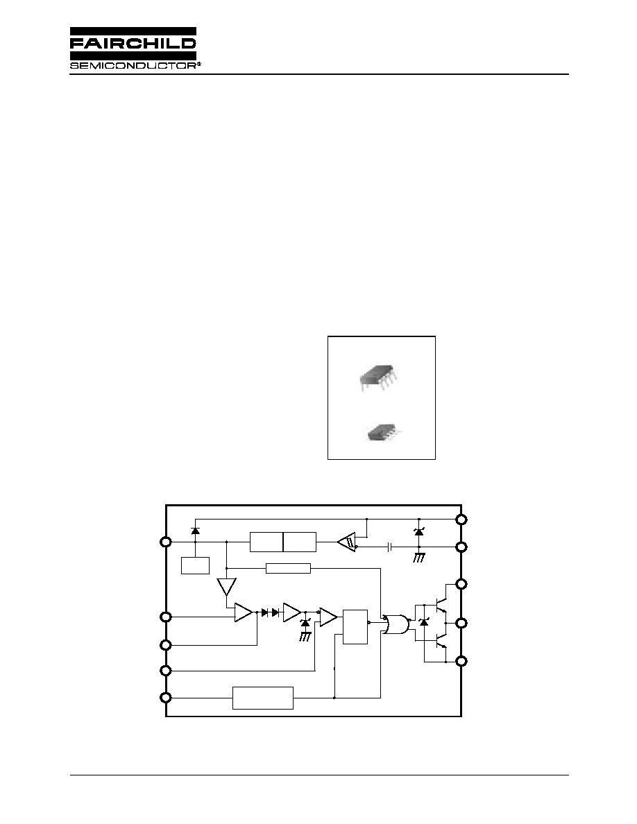
Description
The KA3882C/KA3883C is a fixed PWM controller for Off
Line and DC to DC converter applications. The internal
circuits include an UVLO, a low start up current circuit, a
temperature compensated reference, a high gain error
amplifier, a current sensing comparator, and the high current
totem-pole output for driving a POWER MOSFET. Also the
KA3882C/KA3883C provides low start-up current below
0.3mA and short shutdown delay time typ. 100ns. The
KA3882C has the UVLO threshold of 16V (on) and
10V(off). The KA3883C is 8.4V(on) and 7.6V(off). The
KA3882C and KA3883C can operate within 100% duty
cycle.
8-DIP
8-SOP
1
1
Internal Block Diagram
8
+
-
7
5
SET/
RESET
5V
V
REF
Internal
Bias
Good LOGIC
2
R
S
OSCILLATOR
1
3
4
T
7
6
5
UVLO
29V
22V
1/3
Error Amp
1/2V
REF
1V
C.S
Comp.
PWM
LATCH
V
REF
V
FB
COMP
C.S
R
T
/C
T
OUTPUT
V
CC
GND
PWR
V
C
PWR
GND
KA3882C/KA3883C
SMPS Controller
KA3882C/KA3883C
2
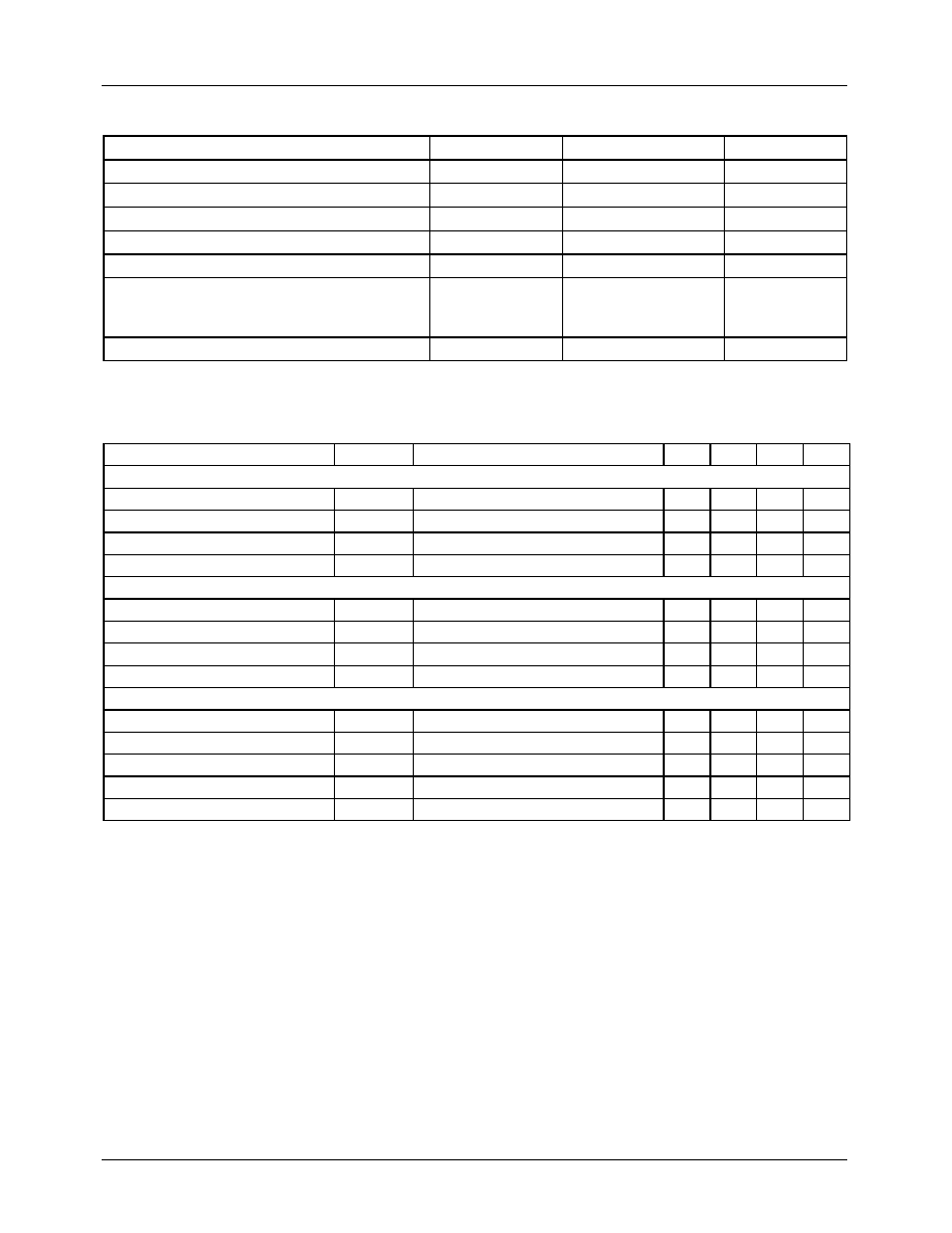
Absolute Maximum Ratings
Electrical Characteristics
(V
CC
= 15V, R
T
= 10k
, C
T
= 3.3nF, T
A
= 0
∞
C to +70
∞
C ,Unless otherwise specified)
Parameter
Symbol
Value
Unit
Supply Voltage
V
CC
30
V
Output Current
I
O
±1
A
Analog Inputs (pin 2, 3)
V
I(ANA)
-0.3 to 6.3
V
Error Amp. Output Sink Current
I
SINK(EA)
10
mA
Power Dissipation
P
D
1
W
Thermal Resistance, Junction-to-Air (Note4)
8-SOP
8-DIP
R
ja
280
95
∞
C/W
Storage Temperature
T
stg
-65 ~ 150
∞
C
Parameter
Symbol
Conditions
Min.
Typ. Max. Unit
REFERENCE SECTION
Output Voltage
V
REF
T
J
= 25
∞
C, I
O
= 1mA
4.9
5.0
5.1
V
Line Regulation
V
REF
V
CC
= 12V to 25V
-
6
20
mV
Load Regulation
V
REF
I
O
= 1mA to 20mA
-
6
25
mV
Output Short Circuit
I
SC
T
a
= 25
∞
C
-
-100
-180
mA
OSILLATOR SECTION
Initial Accuracy
F
OSC
T
J
= 25
∞
C
47
52
57
kHz
Voltage Stability
ST
V
V
CC
= 12V to 25V
-
0.2
1
%
Amplitude
V
OSC
V
PIN4
, Peak to Peak
-
1.7
-
V
Discharge Current
I
DISCHG
T
J
= 25
∞
C, Pin4 = 2V
7.8
8.3
8.8
mA
CURRENT SENSE SECTION
Gain
G
V
(Note2, 3)
2.85
3
3.15
V/V
Maximum Input Signal
V
I(MAX)
V
PIN1
= 5V(Note2)
0.9
1.0
1.1
V
PSRR
PSRR
V
CC
= 12V to 25V (Note1, 2)
-
70
-
dB
Input Bias Current
I
BIAS
-
-
-2
-10
uA
Delay to Output
T
D
V
PIN3
= 0 V to 2V (Note1)
-
100
200
ns
KA3882C/KA3883C
3
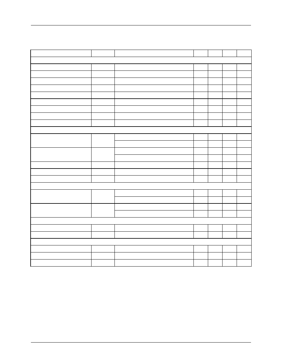
Electrical Characteristics
(Continued)
(V
CC
= 15V, R
T
= 10k
, C
T
= 3.3nF, T
A
= 0
∞
C to +70
∞
C, Unless otherwise specified)
* Adjust V
CC
above the start threshold before setting at 15V
Notes :
1. These parameters, although guaranteed, are not 100% tested in production.
2. Parameter measured at trip point of latch with V2 = 0V.
3. Gain defined as: G
V
=
V
PIN1
V
PIN3
(V
PIN3
= 0 to 0.8V)
4. Junction-to-air thermal resistance test enviroments.
-. PCB information ;
Board thickness : 1.6mm , Board dimension : 76.2 X 114.3mm
2
, Ref. : EIA / JSED51-3 and EIA / JSED51-7
-. Board structure; Using the single layer PCB.
Parameter
Symbol
Conditions
Min.
Typ.
Max.
Unit
ERROR AMPLIFIER SECTION
Input Voltage
V
I
T
PIN1
= 2.5V
2.42
2.50
2.58
V
Input Bias Current
I
BIAS
-
-
-0.3
-2
uA
Open Loop Gain
G
VO
V
O
= 2V to 4V (Note1)
65
90
-
dB
Unity Gain Bandwidth
GBW
T
J
= 25
∞
C
(Note1)
0.7
1
-
MHz
PSRR
PSRR
V
CC
= 12V to 25V (Note1)
60
70
-
dB
Output Sink Current
I
SINK
V
PIN2
= 2.7V, V
PIN1
= 1.1V
2
6
-
mA
Output Source Current
I
SOURCE
V
PIN2
= 2.3V, V
PIN1
= 5.0V
-0.5
-0.8
-
mA
Output High Voltage
V
OH
V
PIN2
= 2.3V, R1 = 15k
to GND
5
6
-
V
Output Low Voltage
V
OL
V
PIN2
= 2.7V, R1 = 15k
to Pin8
-
0.8
1.1
V
OUTPUT SECTION
Output Low Level
V
OL
I
SINK
= 20mA
-
0.1
0.4
V
I
SINK
= 200mA
-
1.5
2.2
V
Output High Level
V
OH
I
SOURCE
= 20mA
13
13.5
-
V
I
SOURCE
= 200mA
12
13.5
-
V
Rise Time
t
R
T
J
= 25
∞
C, C1 = 1nF (Note1)
-
40
100
ns
Fall Time
t
F
T
J
= 25
∞
C, C1 = 1nF (Note1)
-
40
100
ns
Output Voltage Swing Limit
V
OLIM
V
CC
= 27V, C1 = 1nF
-
22
-
V
UNDER VOLTAGE LOCKOUT SECTION
Start Threshold
V
TH
KA3882C
15
16
17
V
KA3883C
7.8
8.4
9.0
V
Min. Operating Voltage
( After turn on )
V
TL
KA3882C
9
10
11
V
KA3883C
7.0
7.6
8.2
V
PWM SECTION
Maximum Duty Cycle
D
MAX
KA3882C/KA3883C
94
96
100
%
Minimum Duty Cycle
D
MIN
-
-
-
0
%
TOTAL STANDBY CURRENT
Start-Up Current
I
ST
-
-
0.2
0.4
mA
Operating Supply Current
I
CC
V
PIN2
= V
PIN3
= 0V
-
11
17
mA
V
CC
Zener Voltage
V
Z
I
CC
= 25mA
-
29
-
V

KA3882C/KA3883C
4
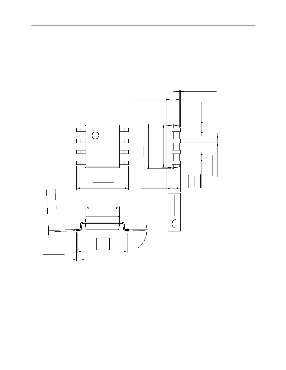
Mechanical Dimensions
Package
6.40
±
0.20
3.30
±
0.30
0.130
±
0.012
3.40
±
0.20
0.134
±
0.008
#1
#4
#5
#8
0.252
±
0.008
9.20
±
0.20
0.79
2.54
0.100
0.031
()
0.46
±
0.10
0.018
±
0.004
0.060
±
0.004
1.524
±
0.10
0.362
±
0.008
9.60
0.378
MAX
5.08
0.200
0.33
0.013
7.62
0~15
∞
0.300
MAX
MIN
0.25
+0.10
≠0.05
0.010
+0.004
≠0.002
8-DIP
KA3882C/KA3883C
5
Mechanical Dimensions
(Continued)
Package
4.92
±
0.20
0.194
±
0.008
0.41
±
0.10
0.016
±
0.004
1.27
0.050
5.72
0.225
1.55
±
0.20
0.061
±
0.008
0.1~0.25
0.004~0.001
6.00
±
0.30
0.236
±
0.012
3.95
±
0.20
0.156
±
0.008
0.50
±
0.20
0.020
±
0.008
5.13
0.202
MAX
#1
#4
#5
0~8
∞
#8
0.56
0.022
()
1.80
0.071
MAX0.10
MAX0.004
MAX
MIN
+
0.10
-0.05
0.15
+
0.004
-0.002
0.006
8-SOP

KA3882C/KA3883C
9/10/02 0.0m 001
Stock#DSxxxxxxxx
"
2002 Fairchild Semiconductor Corporation
LIFE SUPPORT POLICY
FAIRCHILD'S PRODUCTS ARE NOT AUTHORIZED FOR USE AS CRITICAL COMPONENTS IN LIFE SUPPORT DEVICES
OR SYSTEMS WITHOUT THE EXPRESS WRITTEN APPROVAL OF THE PRESIDENT OF FAIRCHILD SEMICONDUCTOR
CORPORATION. As used herein:
1. Life support devices or systems are devices or systems
which, (a) are intended for surgical implant into the body,
or (b) support or sustain life, and (c) whose failure to
perform when properly used in accordance with
instructions for use provided in the labeling, can be
reasonably expected to result in a significant injury of the
user.
2. A critical component in any component of a life support
device or system whose failure to perform can be
reasonably expected to cause the failure of the life support
device or system, or to affect its safety or effectiveness.
www.fairchildsemi.com
DISCLAIMER
FAIRCHILD SEMICONDUCTOR RESERVES THE RIGHT TO MAKE CHANGES WITHOUT FURTHER NOTICE TO ANY
PRODUCTS HEREIN TO IMPROVE RELIABILITY, FUNCTION OR DESIGN. FAIRCHILD DOES NOT ASSUME ANY
LIABILITY ARISING OUT OF THE APPLICATION OR USE OF ANY PRODUCT OR CIRCUIT DESCRIBED HEREIN; NEITHER
DOES IT CONVEY ANY LICENSE UNDER ITS PATENT RIGHTS, NOR THE RIGHTS OF OTHERS.
Ordering Information
Product Number
Package
Operating Temperature
KA3882C
8-DIP
0 ~ +70
∞
C
KA3882CD
8-SOP
KA3883C
8-DIP
KA3883CD
8-SOP