 | –≠–ª–µ–∫—Ç—Ä–æ–Ω–Ω—ã–π –∫–æ–º–ø–æ–Ω–µ–Ω—Ç: KA3883E | –°–∫–∞—á–∞—Ç—å:  PDF PDF  ZIP ZIP |
© 1999 Fairchild Semiconductor Corporation
DS009601
www.fairchildsemi.com
April 1988
Revised August 1999
7
4F845 8-Bi
t T
r
anspa
rent
Lat
ch
74F845
8-Bit Transparent Latch
General Description
The 74F845 bus interface latch is designed to eliminate the
extra packages required to buffer existing latches and pro-
vide extra data width for wider address/data paths or buses
carrying parity.
The 74F845 is functionally- and pin-compatible with AMD's
Am29845.
Features
s
3-STATE outputs
s
Direct replacement for AMD's Am29845
Ordering Code:
Devices also available in Tape and Reel. Specify by appending the suffix letter "X" to the ordering code.
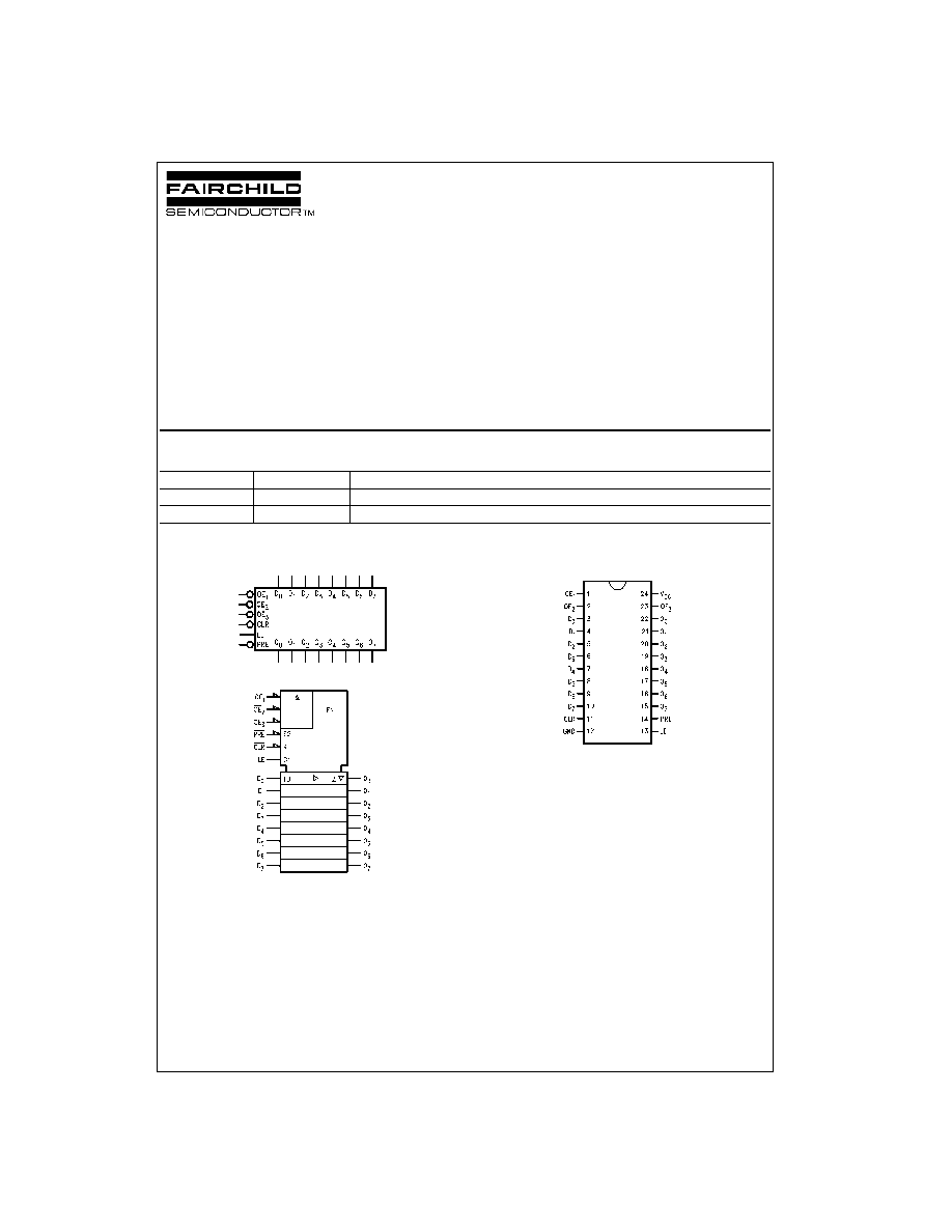
Logic Symbols
IEEE/IEC
Connection Diagram
Order Number
Package Number
Package Description
74F845SC
M24B
24-Lead Small Outline Integrated Circuit (SOIC), JEDEC MS-013, 0.300 Wide
74F845SPC
N24C
24-Lead Plastic Dual-In-Line Package (PDIP), JEDEC MS-100, 0.300 Wide

www.fairchildsemi.com
2
74F845
Unit Loading/Fan Out
Functional Description
The 74F845 consists of eight D-type latches with 3-STATE
outputs. The flip-flops appear transparent to the data when
Latch Enable (LE) is HIGH. This allows asynchronous
operation as the output transition follows the data in transi-
tion. On the LE HIGH-to-LOW transition, the data that
meets the setup times is latched. Data appears on the bus
when the output Enable (OE) is LOW. When OE is HIGH,
the bus output is in the high impedance state.
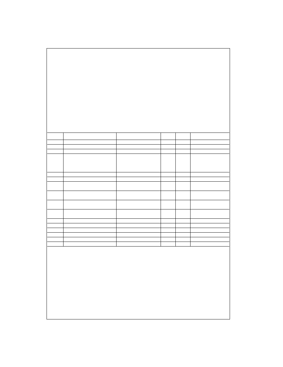
Function Table
H
=
HIGH Voltage Level
Z
=
High Impedance
L
=
LOW Voltage Level
NC
=
No Change
X
=
Immaterial
Logic Diagram
Please note that this diagram is provided only for the understanding of logic operations and should not be used to estimate propagation delays.
Pin Names
Description
U.L.
Input I
IH
/I
IL
HIGH/LOW
Output I
OH
/I
OL
D
0
≠D
7
Data Inputs
1.0/1.0
20
µ
A/
-
0.6 mA
O
0
≠O
7
Data Outputs
150/40
-
3.0
µ
A/24 mA
OE
1
≠OE
3
Output Enables
1.0/1.0
20
µ
A/
-
0.6 mA
LE
Latch Enable
1.0/1.0
20
µ
A/
-
0.6 mA
CLR
Clear
1.0/1.0
20
µ
A/
-
0.6 mA
PRE
Preset
1.0/1.0
20
µ
A/
-
0.6 mA
Inputs
Internal Output
Function
CLR PRE
OE
LE
D
Q
O
H
H
H
X
X
X
Z
High Z
H
H
H
H
L
L
Z
High Z
H
H
H
H
H
H
Z
High Z
H
H
H
L
X
NC
Z
Latched
H
H
L
H
L
L
L
Transparent
H
H
L
H
H
H
H
Transparent
H
H
L
L
X
NC
NC
Latched
H
L
L
X
X
H
H
Preset
L
H
L
X
X
L
L
Clear
L
L
L
X
X
H
H
Preset
L
H
H
L
X
L
Z
Latched
H
L
H
L
X
H
Z
Latched
3
www.fairchildsemi.com
7
4F845
Absolute Maximum Ratings
(Note 1)
Recommended Operating
Conditions
Note 1: Absolute maximum ratings are values beyond which the device
may be damaged or have its useful life impaired. Functional operation
under these conditions is not implied.
Note 2: Either voltage limit or current limit is sufficient to protect inputs.
DC Electrical Characteristics
Storage Temperature
-
65
∞
C to
+
150
∞
C
Ambient Temperature under Bias
-
55
∞
C to
+
125
∞
C
Junction Temperature under Bias
-
55
∞
C to
+
150
∞
C
V
CC
Pin Potential to Ground Pin
-
0.5V to
+
7.0V
Input Voltage (Note 2)
-
0.5V to
+
7.0V
Input Current (Note 2)
-
30 mA to
+
5.0 mA
Voltage Applied to Output
in HIGH State (with V
CC
=
0V)
Standard Output
-
0.5V to V
CC
3-STATE Output
-
0.5V to
+
5.5V
Current Applied to Output
in LOW State (Max)
twice the rated I
OL
(mA)
Free Air Ambient Temperature
0
∞
C to
+
70
∞
C
Supply Voltage
+
4.5V to
+
5.5V
Symbol
Parameter
Min
Typ
Max
Units
V
CC
Conditions
V
IH
Input HIGH Voltage
2.0
V
Recognized as a HIGH Signal
V
IL
Input LOW Voltage
0.8
V
Recognized as a LOW Signal
V
CD
Input Clamp Diode Voltage
-
1.2
V
Min
I
IN
=
-
18 mA
V
OH
Output HIGH
10% V
CC
2.5
I
OH
=
-
1 mA
Voltage
10% V
CC
2.4
V
Min
I
OH
=
-
3 mA
5% V
CC
2.7
I
OH
=
-
1 mA
5% V
CC
2.7
I
OH
=
-
3 mA
V
OL
Output LOW Voltage
10% V
CC
0.5
V
Min
I
OL
=
24 mA
I
IH
Input HIGH Current
5.0
µ
A
Max
V
IN
=
2.7V
I
BVI
Input HIGH Current
7.0
µ
A
Max
V
IN
=
7.0V
Breakdown Test
I
CEX
Output HIGH
50
µ
A
Max
V
OUT
=
V
CC
Leakage Current
V
ID
Input Leakage
4.75
V
0.0
I
ID
=
1.9
µ
A
Test
All Other Pins Grounded
I
OD
Output Leakage
3.75
µ
A
0.0
V
IOD
=
150 mV
Circuit Current
All Other Pins Grounded
I
IL
Input LOW Current
-
0.6
mA
Max
V
IN
=
0.5V
I
OZH
Output Leakage Current
50
µ
A
Max
V
OUT
=
2.7V
I
OZL
Output Leakage Current
-
50
µ
A
Max
V
OUT
=
0.5V
I
OS
Output Short-Circuit Current
-
60
-
150
mA
Max
V
OUT
=
0V
I
ZZ
Bus Drainage Test
500
µ
A
0.0V
V
OUT
=
5.25V
I
CCZ
Power Supply Current
63
85
mA
Max
V
O
=
HIGH Z
www.fairchildsemi.com
4
74F845
AC Electrical Characteristics
AC Operating Requirements
Symbol
Parameter
T
A
=
+
25
∞
C
T
A
=
0
∞
C to
+
70
∞
C
Units
V
CC
=
+
5.0V
V
CC
=
+
5.0V
C
L
=
50 pF
C
L
=
50 pF
Min
Typ
Max
Min
Max
t
PLH
Propagation Delay
2.5
4.8
8.0
2.0
9.0
ns
t
PHL
D
n
to O
n
1.5
3.6
6.5
1.5
7.0
t
PLH
Propagation Delay
5.0
8.1
12.0
4.5
13.5
ns
t
PHL
LE to O
n
2.0
4.4
7.5
2.0
8.0
t
PLH
Propagation Delay
3.0
5.9
10.0
2.5
11.0
ns
PRE to O
n
t
PHL
Propagation Delay
3.0
6.5
10.0
2.5
11.0
ns
CLR to O
n
t
PZH
Output Enable Time
2.5
5.8
9.5
2.0
10.5
ns
t
PZL
OE to O
n
2.5
7.6
12.0
2.0
13.0
t
PHZ
Output Disable Time
1.0
3.1
7.5
1.0
8.5
ns
t
PLZ
OE to O
n
1.0
2.8
6.5
1.0
7.5
Symbol
Parameter
T
A
=
+
25
∞
C
T
A
=
0
∞
C to
+
70
∞
C
Units
V
CC
=
+
5.0V
V
CC
=
+
5.0V
Min
Max
Min
Max
t
S
(H)
Setup Time, HIGH or LOW
2.0
2.5
ns
t
S
(L)
D
n
to LE
2.0
2.5
t
H
(H)
Hold Time, HIGH or LOW
2.5
3.0
ns
t
H
(L)
D
n
to LE
3.0
3.5
t
W
(H)
LE Pulse Width, HIGH
4.0
4.0
ns
t
W
(L)
PRE Pulse Width, LOW
5.0
5.0
ns
t
W
(L)
CLR Pulse Width, LOW
5.0
5.0
ns
t
REC
PRE Recovery Time
10.0
10.0
ns
t
REC
CLR Recovery Time
12.0
13.0
ns

5
www.fairchildsemi.com
7
4F845
Physical Dimensions
inches (millimeters) unless otherwise noted
24-Lead Small Outline Integrated Circuit (SOIC), JEDEC MS-013, 0.300 Wide
Package Number M24B
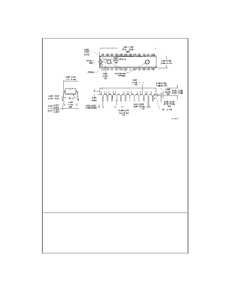
www.fairchildsemi.com
6
74F84
5 8-
Bit
T
r
anspar
ent
Latc
h
Physical Dimensions
inches (millimeters) unless otherwise noted (Continued)
24-Lead Plastic Dual-In-Line Package (PDIP), JEDEC MS-100, 0.300 Wide
Package Number N24C
Fairchild does not assume any responsibility for use of any circuitry described, no circuit patent licenses are implied and
Fairchild reserves the right at any time without notice to change said circuitry and specifications.
LIFE SUPPORT POLICY
FAIRCHILD'S PRODUCTS ARE NOT AUTHORIZED FOR USE AS CRITICAL COMPONENTS IN LIFE SUPPORT
DEVICES OR SYSTEMS WITHOUT THE EXPRESS WRITTEN APPROVAL OF THE PRESIDENT OF FAIRCHILD
SEMICONDUCTOR CORPORATION. As used herein:
1. Life support devices or systems are devices or systems
which, (a) are intended for surgical implant into the
body, or (b) support or sustain life, and (c) whose failure
to perform when properly used in accordance with
instructions for use provided in the labeling, can be rea-
sonably expected to result in a significant injury to the
user.
2. A critical component in any component of a life support
device or system whose failure to perform can be rea-
sonably expected to cause the failure of the life support
device or system, or to affect its safety or effectiveness.
www.fairchildsemi.com