 | –≠–ª–µ–∫—Ç—Ä–æ–Ω–Ω—ã–π –∫–æ–º–ø–æ–Ω–µ–Ω—Ç: KA393AD | –°–∫–∞—á–∞—Ç—å:  PDF PDF  ZIP ZIP |

©2001 Fairchild Semiconductor Corporation
www.fairchildsemi.com
Rev. 1.0.2
Features
∑ Single Supply Operation: 2V to 36V
∑ Dual Supply Operation:
±
1V to
±
18V
∑ Allow Comparison of Voltages Near Ground Potential
∑ Low Current Drain 800
µ
A Typ.
∑ Compatible with all Forms of Logic
∑ Low Input Bias Current 25nA Typ.
∑ Low Input Offset Current
±
5nA Typ.
∑ Low Offset Voltage
±
1mV Typ.
Descritpion
The KA293 series consists of two independent voltage
comparators designed to operate from a single power supply
over a wide voltage range.
8-DIP
8-SOP
9-SIP
1
1
1
Internal Block Diagram
KA293/KA293A, KA393/KA393A,
KA2903
Dual Differential Comparator
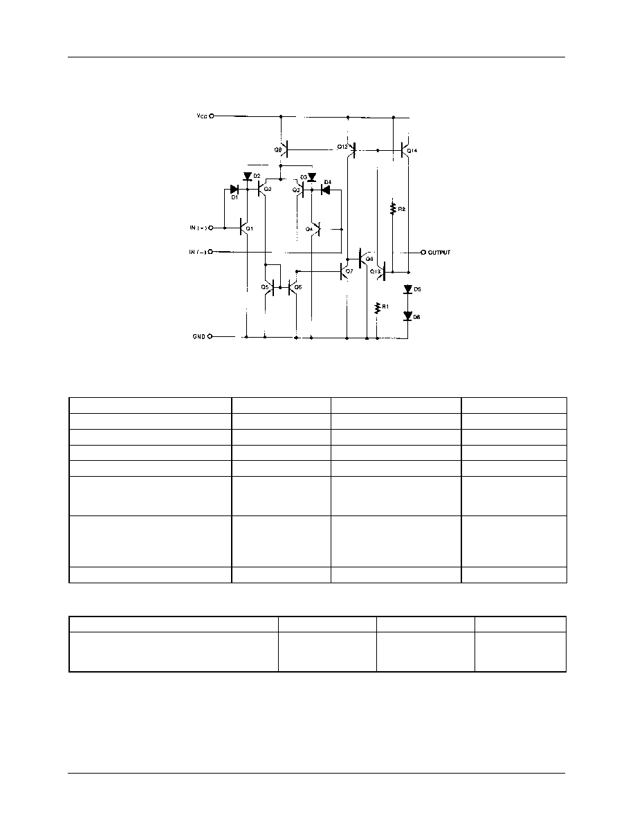
KA293/KA293A, KA393/KA393A, KA2903
2
Schematic Diagram
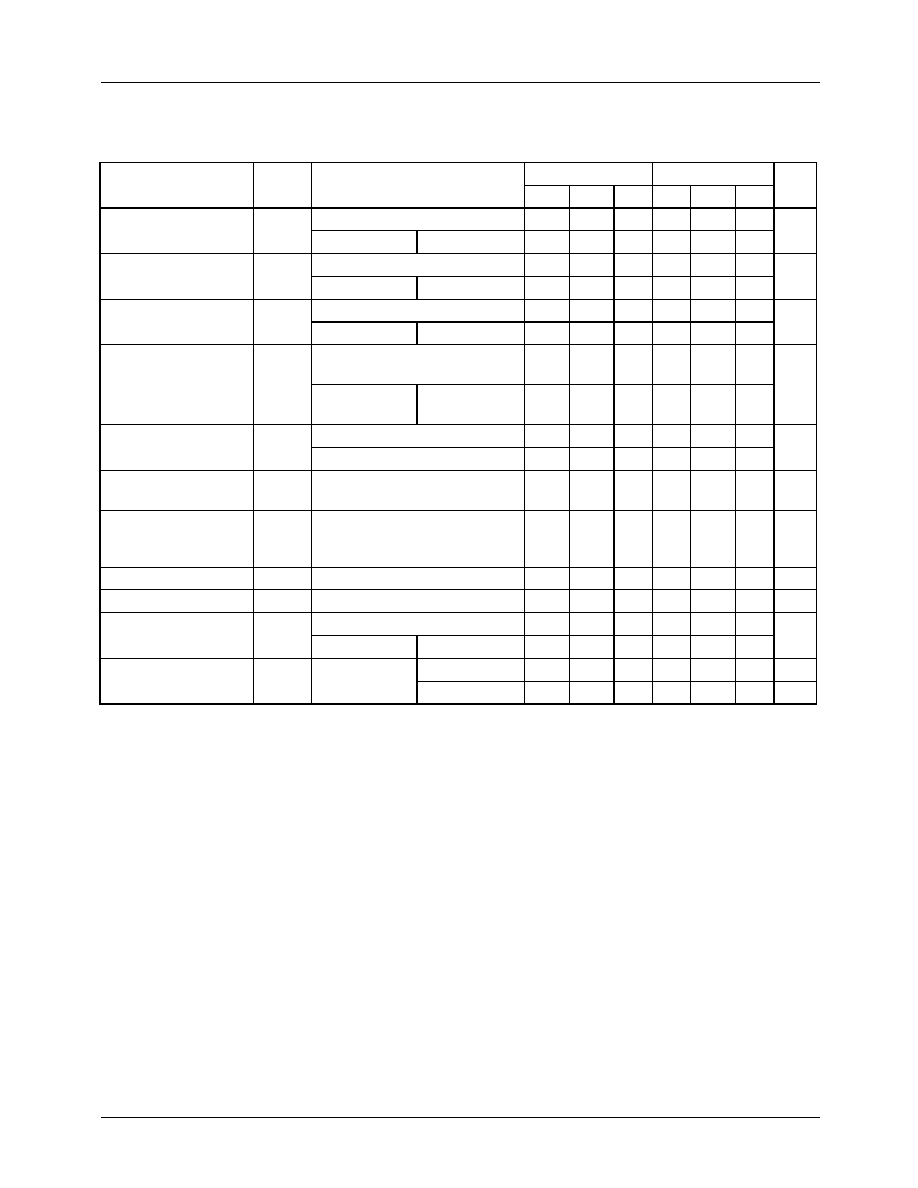
Absolute Maximum Ratings
Thermal Data
Parameter
Symbol
Value
Unit
Power Supply Voltage
V
CC
±
18 or 36
V
Differential Input Voltage
V
I(DIFF)
36
V
Input Voltage
V
I
- 0.3 to +36
V
Output Short Circuit to GND
-
Continuous
-
Power Dissipation, Ta = 25
∞
C
8-DIP
8-SOP
P
D
1040
480
mW
Operating Temperature
KA393/KA393A
KA293/KA293A
KA2903
T
OPR
0 ~ + 70
- 25 ~ + 85
- 40 ~ + 85
∞
C
Storage Temperature
T
STG
- 65 ~ + 150
∞
C
Parameter
Symbol
Value
Unit
Thermal Resistance Junction-Ambient Max.
8-DIP
8-SOP
R
ja
120
260
∞
C/W
KA293/KA293A, KA393/KA393A, KA2903
3
Electrical Characteristics
(V
CC
=5V, T
A
=25
∞
C, unless otherwise specified)
NOTE 1
KA393 / KA393A : 0
T
A
+70
∞
C
KA293 / KA293A : -25
T
A
+85
∞
C
KA2903 : -40
T
A
+85
∞
C
Parameter
Symbol
Conditions
KA293A/KA393A
KA293/KA393
Unit
Min.
Typ. Max. Min. Typ. Max.
Input Offset Voltage
V
IO
V
O(P)
=1.4V, R
S
=0
-
±
1
±
2
-
±
1
±
5
mV
V
CM
= 0 to1.5V Note 1
-
-
±
4.0
-
-
±
9.0
Input Offset Current
I
IO
-
±
5
±
50
-
±
5
±
50
nA
Note 1
-
-
±
150
-
-
±
150
Input Bias Current
I
BIAS
-
65
250
-
65
250
nA
Note 1
-
-
400
-
-
400
Input Common Mode
Voltage Range
V
I(R)
0
-
V
CC
-1.5
0
-
V
CC
-1.5
V
Note 1
0
-
V
CC
-2
0
-
V
CC
-2
Supply Current
I
CC
R
L
=
,
V
CC
= 5V
-
0.6
1
-
0.6
1
mA
R
L
=
, V
CC
= 30V
-
0.8
2.5
-
0.8
2.5
Voltage Gain
G
V
V
CC
=15V, R
L
15K
(for large V
O(P-P)swing
)
50
200
-
50
200
-
V/mV
Large Signal
Response
Time
T
LRES
V
I
=TTL Logic Swing
V
REF
=1.4V, V
RL
=5V,
R
L
=5.1K
-
350
-
-
350
-
nS
Response Time
T
RES
V
RL
=5V, R
L
=5.1K
-
1.4
-
-
1.4
-
µ
S
Output Sink Current
I
SINK
V
I(-)
1V, V
I(+)
=0V, V
O(P)
1.5V
6
18
-
6
18
-
mA
Output Saturation
Voltage
V
SAT
V
I(-)
1V, VI(+) =0V
-
160
400
-
160
400
mV
I
SINK
= 4mA
Note 1
-
-
700
-
-
700
Output Leakage
Current
I
O(LKG)
V
I(-)
= 0V,
V
I(+)
= 1V
V
O(P)
= 5V
-
0.1
-
-
0.1
-
nA
V
O(P)
= 30V
-
-
1.0
-
-
1.0
µ
A
KA293/KA293A, KA393/KA393A, KA2903
4
Electrical Characteristics
(Continued)
(V
CC
=5V, T
A
=25
∞
C, unless otherwise specified)
NOTE 1
KA393 / KA393A : 0
T
A
+70
∞
C
KA293 / KA293A : -25
T
A
+85
∞
C
KA2903 : -40
T
A
+85
∞
C
Parameter
Symbol
Conditions
KA2903
Unit
Min.
Typ.
Max.
Input Offset Voltage
V
IO
V
O(P)
=1.4V, R
S
=0
-
±
1
±
7
mV
V
CM
= 0 to 1.5V
Note 1
-
±
9
±
15
Input Offset Current
I
IO
-
±
5
±
50
nA
Note 1
-
±
50
±
200
Input Bias Current
I
BIAS
-
65
250
nA
Note 1
-
-
500
Input Common Mode
Voltage Range
V
I(R)
0
-
V
CC
-1.5
V
Note 1
0
-
V
CC
-2
Supply Current
I
CC
R
L
=
,
V
CC
= 5V
-
0.6
1
mA
R
L
=
, V
CC
= 30V
-
1
2.5
Voltage Gain
G
V
V
CC
=15V, R
L
15K
(for large
V
O(P-P)swing
)
25
100
-
V/mV
Large Signal Response Time
T
LRES
V
I
=TTL Logic Swing
V
REF
=1.4V, V
RL
=5V, R
L
=5.1K
-
350
-
nS
Response Time
T
RES
V
RL
=5V, R
L
=5.1K
-
1.5
-
µ
S
Output Sink Current
I
SINK
V
I(-)
1V, V
I(+)
=0V, V
O(P)
1.5V
6
16
-
mA
Output Saturation Voltage
V
SAT
V
I(-)
1V, VI(+) =0V
-
160
400
mV
I
SINK
= 4mA
NOTE 1
-
-
700
Output Leakage Current
I
O(LKG)
V
I(-)
= 0V,
V
O(P)
= 5V
-
0.1
-
nA
V
I(+)
= 1V
V
O(P)
= 30V
-
-
1.0
µ
A
KA293/KA293A, KA393/KA393A, KA2903
5
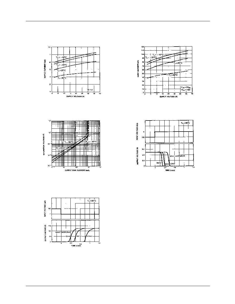
Typical Performance Characteristics
Figure 1. Supply Current vs Supply Voltage
Figure 2. Input Current vs Supply Voltage
Figure 3. Output Saturation Voltage vs Sink Current
Figure 4. Response Time for Various Input
Overdrive-Negative Transition
Figure 5. Response Time for Various Input
Overdrive-Positive Transition
KA293/KA293A, KA393/KA393A, KA2903
6
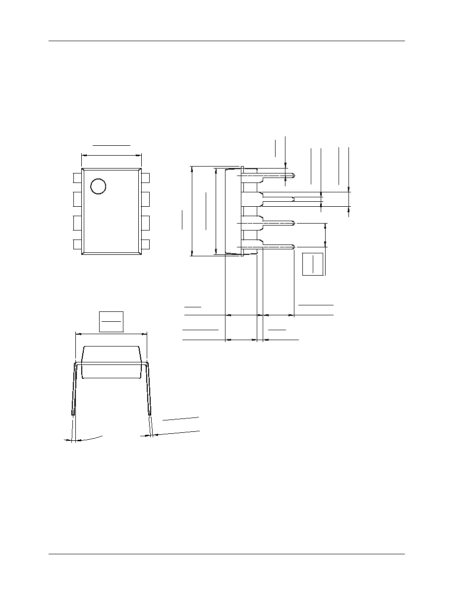
Mechanical Dimensions
Package
Dimensions in millimeters
6.40
±
0.20
3.30
±
0.30
0.130
±
0.012
3.40
±
0.20
0.134
±
0.008
#1
#4
#5
#8
0.252
±
0.008
9.20
±
0.20
0.79
2.54
0.100
0.031
()
0.46
±
0.10
0.018
±
0.004
0.060
±
0.004
1.524
±
0.10
0.362
±
0.008
9.60
0.378
MAX
5.08
0.200
0.33
0.013
7.62
0~15
∞
0.300
MAX
MIN
0.25
+0.10
≠0.05
0.010
+0.004
≠0.002
8-DIP

KA293/KA293A, KA393/KA393A, KA2903
7
Mechanical Dimensions
(Continued)
Package
Dimensions in millimeters
4.92
±
0.20
0.194
±
0.008
0.41
±
0.10
0.016
±
0.004
1.27
0.050
5.72
0.225
1.55
±
0.20
0.061
±
0.008
0.1~0.25
0.004~0.001
6.00
±
0.30
0.236
±
0.012
3.95
±
0.20
0.156
±
0.008
0.50
±
0.20
0.020
±
0.008
5.13
0.202
MAX
#1
#4
#5
0~8
∞
#8
0.56
0.022
()
1.80
0.071
MAX0.10
MAX0.004
MAX
MIN
+
0.10
-0.05
0.15
+
0.004
-0.002
0.006
8-SOP

KA293/KA293A, KA393/KA393A, KA2903
8
Mechanical Dimensions
(Continued)
Package
Dimensions in millimeters
21.84
±
0.20
0.860
±
0.008
22.24
0.876
MAX
1.20
±
0.10
0.047
±
0.004
0.60
±
0.10
0.024
±
0.004
0.76
0.030
()
2.54
0.100
1.15
±
0.20
0.045
±
0.008
5.80
±
0.20
0.228
±
0.008
3.30
±
0.30
0.130
±
0.012
7.30
0.287
MAX
#1
#9
1.25
±
0.10
3.00
±
0.20
0.118
±
0.008
0.049
±
0.004
0.25
±
0.10
0.010
±
0.004
6.00
0.236
MAX
9-SIP
KA293/KA293A, KA393/KA393A, KA2903
9
Ordering Information
Product Number
Package
Operating Temperature
KA393
8-DIP
0 ~ + 70
∞
C
KA393A
KA393D
8-SOP
KA393AD
KA393S
9-SIP
KA293
8-DIP
-25 ~ + 85
∞
C
KA293A
KA293D
8-SOP
KA293AD
KA2903
8-DIP
-40 ~ + 85
∞
C
KA2903D
8-SOP

KA293/KA293A, KA393/KA393A, KA2903
12/21/01 0.0m 001
Stock#DSxxxxxxxx
2001 Fairchild Semiconductor Corporation
LIFE SUPPORT POLICY
FAIRCHILD'S PRODUCTS ARE NOT AUTHORIZED FOR USE AS CRITICAL COMPONENTS IN LIFE SUPPORT DEVICES
OR SYSTEMS WITHOUT THE EXPRESS WRITTEN APPROVAL OF THE PRESIDENT OF FAIRCHILD SEMICONDUCTOR
CORPORATION. As used herein:
1. Life support devices or systems are devices or systems
which, (a) are intended for surgical implant into the body,
or (b) support or sustain life, and (c) whose failure to
perform when properly used in accordance with
instructions for use provided in the labeling, can be
reasonably expected to result in a significant injury of the
user.
2. A critical component in any component of a life support
device or system whose failure to perform can be
reasonably expected to cause the failure of the life support
device or system, or to affect its safety or effectiveness.
www.fairchildsemi.com
DISCLAIMER
FAIRCHILD SEMICONDUCTOR RESERVES THE RIGHT TO MAKE CHANGES WITHOUT FURTHER NOTICE TO ANY
PRODUCTS HEREIN TO IMPROVE RELIABILITY, FUNCTION OR DESIGN. FAIRCHILD DOES NOT ASSUME ANY
LIABILITY ARISING OUT OF THE APPLICATION OR USE OF ANY PRODUCT OR CIRCUIT DESCRIBED HEREIN; NEITHER
DOES IT CONVEY ANY LICENSE UNDER ITS PATENT RIGHTS, NOR THE RIGHTS OF OTHERS.