©2001 Fairchild Semiconductor Corporation
www.fairchildsemi.com
Rev.1.0.1
Features
∑ Wide operating frequency range up to 150KHz
∑ Pulse by pulse over current limiting
∑ Over current protection
∑ Over voltage protection (Min. 23V)
∑ Internal thermal shutdown function
∑ Under voltage lockout
∑ Internal high voltage sense FET
∑ External sync terminal
∑ Auto Restart Mode
Description
The SPS product family is specially designed for an off-line
SMPS with minimal external components. The SPS consist of
high voltage power SenseFET and current mode PWM Control-
ler IC. PWM controller features integrated fixed oscillator,
under voltage lock out, leading edge blanking, optimized gate
turn-on/turn-off driver, thermal shut down protection, over volt-
age protection, temperature compensated precision current
sources for loop compensation and fault protection circuit.
Compared to discrete MOSFET and controller or RCC switch-
ing converter solution, a SPS can reduce total component count,
design size, weight and at the same time increase & efficiency,
productivity, and system reliability. It has a basic platform well
suited for cost effective design in C-TV power supply.
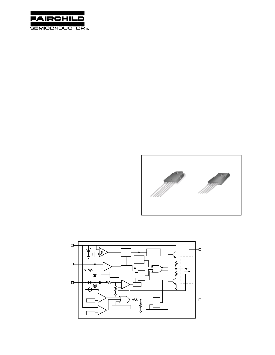
TO-3PF-5L
1. DRAIN 2. GND 3. V
CC
4. FB 5. Sync
TO-3P-5L
1
1
Internal Block Diagram
#3 V
CC
32V
2
µ
A
5V
2.5R
1R
1mA
0.1V
+
-
OVER VOLTAGE S/D
+
-
7.5V
25V
Thermal S/D
S
R
Q
Power on reset
+
-
L.E.B
S
R
Q
OSC
5V
Vref
Internal
bias
Good
logic
SFET
#1 DRAIN
#2 GND
#4 FB
#5 Sync
9V
+
-
6.4V
KA3S0880RB/KA3S0880RFB
Fairchild Power Switch(SPS)

KA3S0880RB/KA3S0880RFB
2
Absolute Maximum Ratings
Notes:
1. Tj=25
∞
C to 150
∞
C
2. Repetitive rating: Pulse width limited by maximum junction temperature
3. L=24mH, starting Tj=25
∞
C
4. L=13
µ
H, starting Tj=25
∞
C
Parameter
Symbol
Value
Unit
Maximum Drain voltage
(1)
V
D,MAX
800
V
Drain-Gate voltage (R
GS
=1M
)
V
DGR
800
V
Gate-source (GND) voltage
V
GS
±
30
V
Drain current pulsed
(2)
I
DM
32.0
A
DC
Single pulsed avalanche energy
(3)
E
AS
810
mJ
Avalanche current
(4)
I
AS
25
A
Continuous drain current (T
C
=25
∞
C)
I
D
8.0
A
DC
Continuous drain current (T
C
=100
∞
C)
I
D
5.6
A
DC
Maximum supply voltage
V
CC,MAX
30
V
Input voltage range
V
FB
-
0.3 to V
SD
V
Total power dissipation
P
D
190
W
Derating
1.54
W/
∞
C
Operating ambient temperature
T
A
-
25 to +85
∞
C
Storage temperature
T
STG
-
55 to +150
∞
C
KA3S0880RB/KA3S0880RFB
3
Electrical Characteristics (SFET part)
(Ta=25
∞
C unless otherwise specified)
Note:
Pulse test: Pulse width
300
µ
S, duty cycle
2%
Parameter
Symbol
Condition
Min.
Typ.
Max.
Unit
Drain-source breakdown voltage
BV
DSS
V
GS
=0V, I
D
=50
µ
A
800
-
-
V
Zero gate voltage drain current
I
DSS
V
DS
=Max., Rating,
V
GS
=0V
-
-
50
µ
A
V
DS
=0.8Max., Rating,
V
GS
=0V, T
C
=125
∞
C
-
-
200
µ
A
Static drain-source on resistance
(note)
R
DS(ON)
V
GS
=10V, I
D
=5.0A
-
1.2
1.5
Forward transconductance
(note)
gfs
V
DS
=15V, I
D
=5.0A
1.5
2.5
-
S
Input capacitance
Ciss
V
GS
=0V, V
DS
=25V,
f=1MHz
-
2460
-
pF
Output capacitance
Coss
-
210
-
Reverse transfer capacitance
Crss
-
64
-
Turn on delay time
td(on)
V
DD
=0.5BV
DSS
, I
D
=8.0A
(MOSFET switching
time are essentially
independent of
operating temperature)
-
-
90
nS
Rise time
tr
-
95
200
Turn off delay time
td(off)
-
150
450
Fall time
tf
-
60
150
Total gate charge
(gate-source+gate-drain)
Qg
V
GS
=10V, I
D
=8.0A,
V
DS
=0.5BV
DSS
(MOSFET
switching time are
essentially independent of
operating temperature)
-
-
150
nC
Gate-source charge
Qgs
-
20
-
Gate-drain (Miller) charge
Qgd
-
70
-
S
1
R
----
=

KA3S0880RB/KA3S0880RFB
4
Electrical Characteristics (Control part)
(Ta=25
∞
C unless otherwise specified)
Notes:
1. These parameters, although guaranteed, are not 100% tested in production
2. These parameters, although guaranteed, are tested in EDS (wafer test) process
3. The amplitude of the sync. pulse is recommended to be between 2V and 3V for stable sync. function.
Parameter
Symbol
Condition
Min.
Typ.
Max.
Unit
UVLO SECTION
Start threshold voltage
V
START
-
14
15
16
V
Stop threshold voltage
V
STOP
After turn on
9
10
11
V
OSCILLATOR SECTION
Initial accuracy
F
OSC
Ta=25
∞
C
18
20
22
kHz
Frequency change with temperature
(2)
F/
T
-
25
∞
C
Ta
+85
∞
C
-
±
5
±
10
%
Maximum duty cycle
Dmax
-
92
95
98
%
FEEDBACK SECTION
Feedback source current
I
FB
Ta=25
∞
C, Vfb=GND
0.7
0.9
1.1
mA
Shutdown Feedback voltage
V
SD
-
6.9
7.5
8.1
V
Shutdown delay current
Idelay
Ta=25
∞
C, 5V
Vfb
V
SD
1.4
1.8
2.2
µ
A
SYNC. & SOFT START SECTION
Soft start voltage
V
SS
V
FB
=2V
4.7
5.0
5.3
V
Soft start current
I
SS
Sync & S/S=GND
0.8
1.0
1.2
mA
Sync threshold voltage
(3)
V
SYTH
Vfb=5V
6.0
6.4
6.8
V
REFERENCE SECTION
Output voltage
(1)
Vref
Ta=25
∞
C
4.80
5.00
5.20
V
Temperature Stability
(1)(2)
Vref/
T
-
25
∞
C
Ta
+85
∞
C
-
0.3
0.6
mV/
∞
C
CURRENT LIMIT (SELF-PROTECTION) SECTION
Peak Current Limit
I
OVER
Max. inductor current
4.40
5.00
5.60
A
PROTECTION SECTION
Thermal shutdown temperature (Tj)
(1)
T
SD
-
140
160
-
∞
C
Over voltage protection voltage
V
OVP
-
23
25
28
V
TOTAL DEVICE SECTION
Start Up current
I
START
V
CC
=14V
0.1
0.3
0.55
mA
Operating supply current
(control part only)
I
OP
Ta=25
∞
C
6
12
18
mA
V
CC
zener voltage
V
Z
I
CC
=20mA
30
32.5
35
V
KA3S0880RB/KA3S0880RFB
5
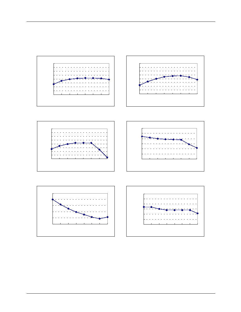
Typical Performance Characteristics
(These characteristic graphs are normalized at Ta=25
∞
C)
Fig.1 Operating Frequency
0.8
0.85
0.9
0.95
1
1.05
1.1
1.15
1.2
-25
0
25
50
75
100 125 150
Fosc
Fig.2 Feedback Source Current
0.8
0.85
0.9
0.95
1
1.05
1.1
1.15
1.2
-25
0
25
50
75
100 125 150
Ifb
Fig.3 Operating Current
0.8
0.85
0.9
0.95
1
1.05
1.1
1.15
1.2
-25
0
25
50
75
100 125 150
Iop
Fig.4 Max Inductor Current
0.8
0.85
0.9
0.95
1
1.05
1.1
-25
0
25
50
75
100 125 150
Ipeak
Fig.5 Start up Current
0.5
0.7
0.9
1.1
1.3
1.5
-25
0
25
50
75
100 125 150
Istart
Fig.6 Start Threshold Voltage
0.85
0.9
0.95
1
1.05
1.1
1.15
-25
0
25
50
75 100 125 150
Vstart
Temperature [
∞
C
]
Temperature [
∞
C
]
Temperature [
∞
C
]
Temperature [
∞
C
]
Temperature [
∞
C
]
Temperature [
∞
C
]
Figure 1. Operating Frequency
Figure 2. Feedback Source Current
Figure 3. Operating Supply Current
Figure 4. Peak Current Limit
Figure 5. Start up Current
Figure 6. Start Threshold Voltage
I
over