©2003 Fairchild Semiconductor Corporation
www.fairchildsemi.com
Rev.1.0.4
Features
∑ Precision Fixed Operating Frequency (100/67/50kHz)
∑ Low Start-up Current (Typ. 100uA)
∑ Pulse by Pulse Current Limiting
∑ Over Load Protection
∑ Over Voltage Protection (Min. 25V)
∑ Internal Thermal Shutdown Function
∑ Under Voltage Lockout
∑ Internal High Voltage Sense FET
∑ Auto-Restart Mode
Description
The Fairchild Power Switch(FPS) product family is specially
designed for an off-line SMPS with minimal external
components. The Fairchild Power Switch(FPS) consist of high
voltage power SenseFET and current mode PWM IC. Included
PWM controller features integrated fixed oscillator, under
voltage lock out, leading edge blanking, optimized gate turn-on/
turn-off driver, thermal shut down protection, over voltage
protection, and temperature compensated precision current
sources for loop compensation and fault protection circuitry-
compared to discrete MOSFET and controller or R
CC
switching converter solution. The Fairchild Power Switch(FPS)
can reduce total component count, design size, weight and at the
same time increase efficiency, productivity, and system
reliability. It has a basic platform well suited for cost-effective
design in either a flyback converter or a forward converter.
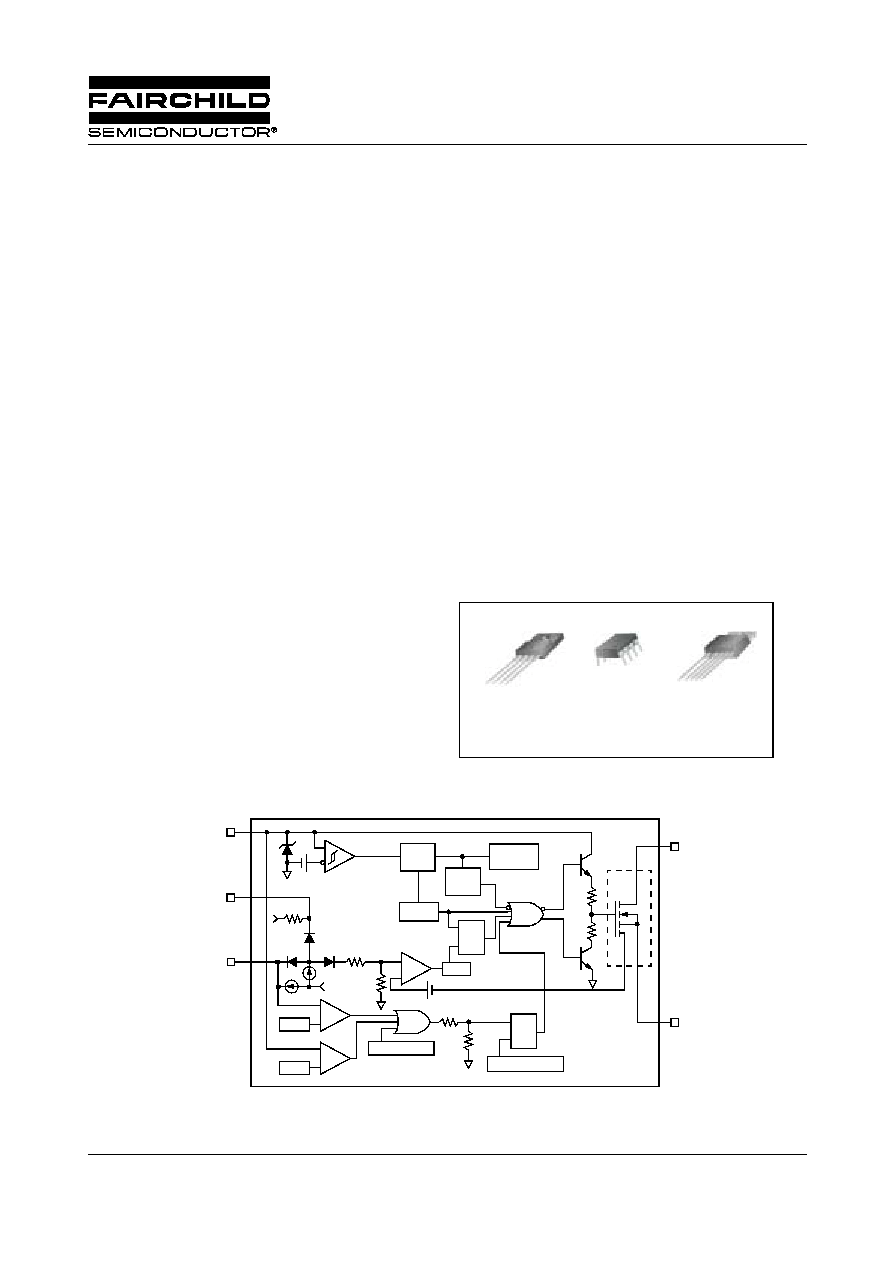
TO-220F-4L
8-DIP
TO220-5L
1
1
1
1. Drain
2. GND
3. Vcc
4. FB
5. S/S
1.6.7.8. Drain
2. GND
3. Vcc
4. FB
5. NC
1. GND
2. Drain
3. Vcc
4. FB
uA
Internal Block Diagram
V
CC
32V
5
µ
A
5V
2.5R
1R
1mA
0.1V
+
-
OVER VOLTAGE S/D
+
-
7.5V
27V
Thermal S/D
S
R
Q
Power on reset
+
-
L.E.B
S
R
Q
OSC
5V
Vref
Internal
bias
Good
logic
SFET
DRAIN
GND
FB
Soft Start
9V
*
* KA5H0265RC
KA5x02xx-SERIES
KA5H0265RC, KA5M0265R, KA5L0265R,
KA5H02659RN/KA5M02659RN, KA5H0280R,
KA5M0280R
Fairchild Power Switch(FPS)
KA5X02XX-SERIES
2
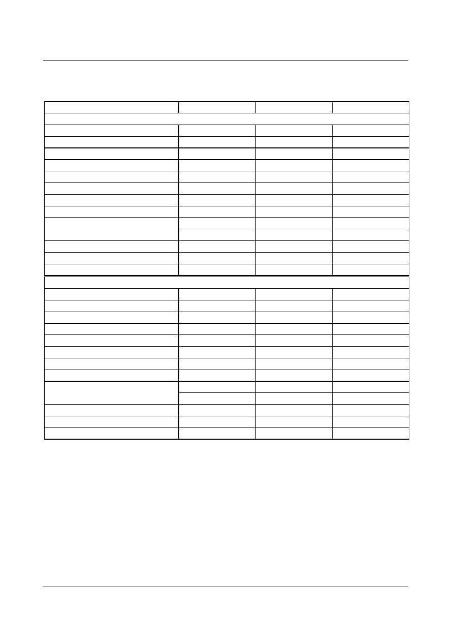
Absolute Maximum Ratings
(Ta=25
∞
C, unless otherwise specified)
Note:
1. Repetitive rating: Pulse width limited by maximum junction temperature
2. L =
51mH, starting T
j
=
25
∞
C
Characteristic
Symbol
Value
Unit
KA5x0265xRx
Drain-Gate Voltage (R
GS
=1M
)
V
DGR
650
V
Gate-Source (GND) Voltage
V
GS
±
30
V
Drain Current Pulsed
(1)
I
DM
8.0
A
DC
Continuous Drain Current (T
C
=25
∞
C)
I
D
2.0
A
DC
Continuous Drain Current (T
C
=100
∞
C)
I
D
1.3
A
DC
Single Pulsed Avalanche Energy
(2)
E
AS
68
mJ
Maximum Supply Voltage
V
CC,MAX
30
V
Analog Input Voltage Range
V
FB
-0.3 to V
SD
V
Total Power Dissipation
P
D
42
W
Darting
0.33
W/
∞
C
Operating Junction Temperature.
T
J
+160
∞
C
Operating Ambient Temperature.
T
A
-25 to +85
∞
C
Storage Temperature Range.
T
STG
-55 to +150
∞
C
KA5x0280R
Drain-Gate Voltage (R
GS
=1M
)
V
DGR
800
V
Gate-Source (GND) Voltage
V
GS
±
30
V
Drain Current Pulsed
(1)
I
DM
8.0
A
DC
Continuous Drain Current (T
C
=25
∞
C)
I
D
2.0
A
DC
Continuous Drain Current (T
C
=100
∞
C)
I
D
1.3
A
DC
Single Pulsed Avalanche Energy
(2)
E
AS
90
mJ
Maximum Supply Voltage
V
CC,MAX
30
V
Analog Input Voltage Range
V
FB
-0.3 to V
SD
V
Total Power Dissipation
P
D
35
W
Darting
0.28
W/
∞
C
Operating Junction Temperature.
T
J
+160
∞
C
Operating Ambient Temperature.
T
A
-25 to +85
∞
C
Storage Temperature Range.
T
STG
-55 to +150
∞
C
KA5X02XX-SERIES
3
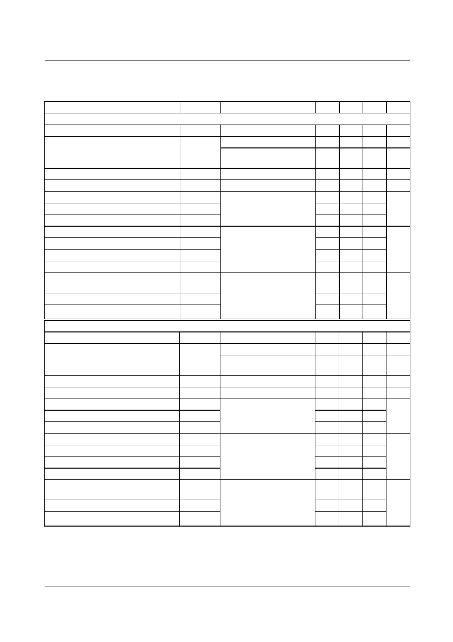
Electrical Characteristics (SFET Part)
(Ta=25
∞
C unless otherwise specified)
Note:
1.
Pulse test: Pulse width
300
µ
S, duty cycle
2%
2.
Parameter
Symbol
Condition
Min.
Typ.
Max.
Unit
KA5x0265xRx
Drain-Source Breakdown Voltage
BV
DSS
V
GS
=0V, I
D
=50
µ
A
650
-
-
V
Zero Gate Voltage Drain Current
I
DSS
V
DS
=Max. Rating, V
GS
=0V
-
-
50
µ
A
V
DS
=0.8Max. Rating,
V
GS
=0V, T
C
=125
∞
C
-
-
200
µ
A
Static Drain-Source on Resistance
(Note)
R
DS(ON)
V
GS
=10V, I
D
=0.5A
-
5.0
6.0
Forward Transconductance
(Note)
gfs
V
DS
=50V, I
D
=0.5A
1.5
2.5
-
S
Input Capacitance
Ciss
V
GS
=0V, V
DS
=25V,
f=1MHz
-
550
-
pF
Output Capacitance
Coss
-
38
-
Reverse Transfer Capacitance
Crss
-
17
-
Turn on Delay Time
td(on)
V
DD
=0.5B V
DSS
, I
D
=1.0A
(MOSFET switching time is
essentially independent of
operating temperature)
-
20
-
nS
Rise Time
tr
-
15
-
Turn Off Delay Time
td(off)
-
55
-
Fall Time
tf
-
25
-
Total Gate Charge
(Gate-Source+Gate-Drain)
Qg
V
GS
=10V, I
D
=1.0A,
V
DS
=0.5B V
DSS
(MOSFET
switching time is essentially
independent of operating
temperature)
-
-
35
nC
Gate-Source Charge
Qgs
-
3
-
Gate-Drain (Miller) Charge
Qgd
-
12
-
KA5x0280R
Drain-Source Breakdown Voltage
BV
DSS
V
GS
=0V, I
D
=50
µ
A
800
-
-
V
Zero Gate Voltage Drain Current
I
DSS
V
DS
=Max. Rating, V
GS
=0V
-
-
50
µ
A
V
DS
=0.8Max. Rating,
V
GS
=0V, T
C
=125
∞
C
-
-
200
µ
A
Static Drain-Source on Resistance
(Note)
R
DS(ON)
V
GS
=10V, I
D
=0.5A
-
5.6
7.0
Forward Transconductance
(Note)
gfs
V
DS
=50V, I
D
=0.5A
1.5
2.5
-
S
Input Capacitance
Ciss
V
GS
=0V, V
DS
=25V,
f=1MHz
-
250
-
pF
Output Capacitance
Coss
-
52
-
Reverse Transfer Capacitance
Crss
-
25
-
Turn on Delay Time
td(on)
V
DD
=0.5B V
DSS
, I
D
=1.0A
(MOSFET switching time is
essentially independent of
operating temperature)
-
21
-
nS
Rise Time
tr
-
28
-
Turn Off Delay Time
td(off)
-
77
-
Fall Time
tf
-
24
-
Total Gate Charge
(Gate-Source+Gate-Drain)
Qg
V
GS
=10V, I
D
=1.0A,
V
DS
=0.5B V
DSS
(MOSFET
switching time is essentially
independent of operating
temperature)
-
-
60
nC
Gate-Source Charge
Qgs
-
15
-
Gate-Drain (Miller) Charge
Qgd
-
20
-
S
1
R
----
=
KA5X02XX-SERIES
4
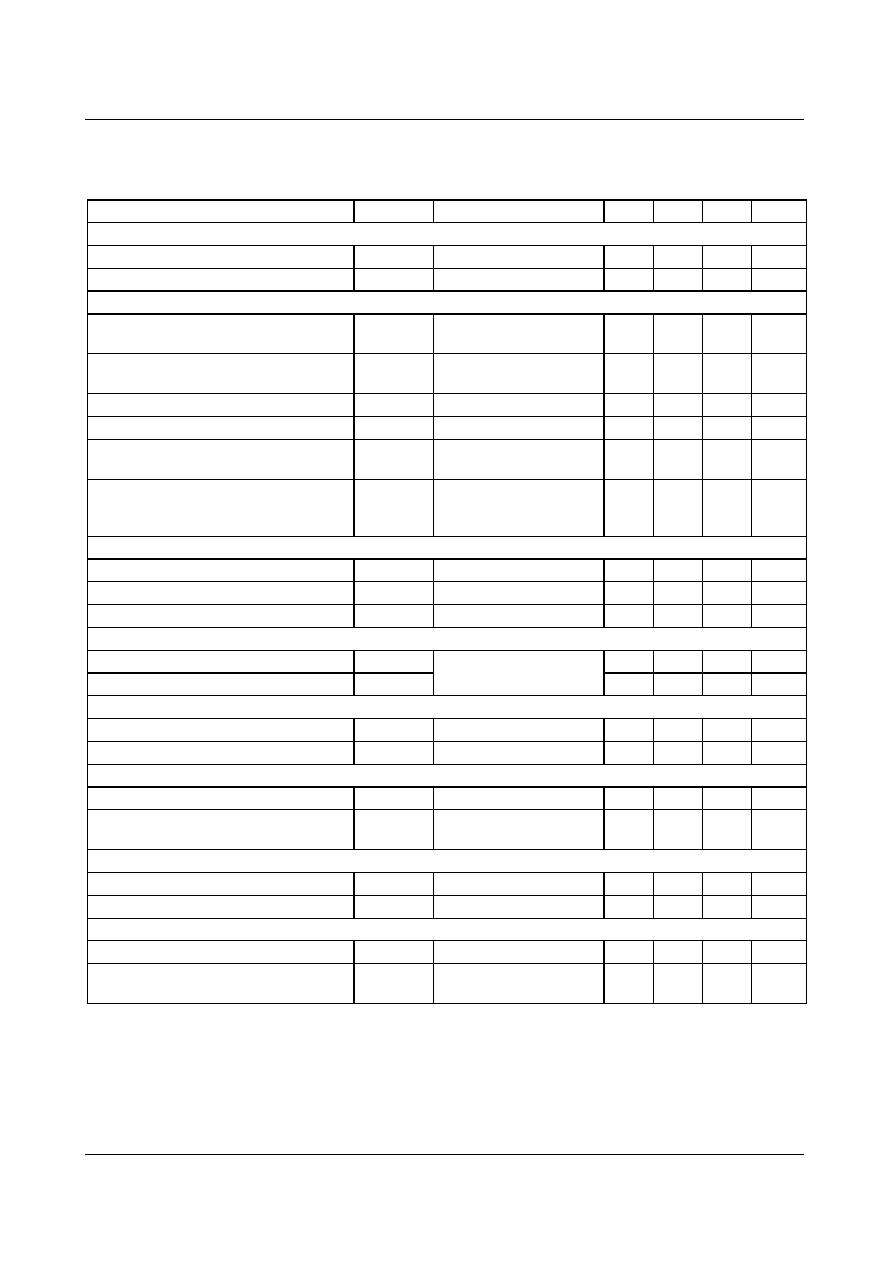
Electrical Characteristics (Control Part)
(Continued)
(Ta=25
∞
C unless otherwise specified)
Note:
1.
These parameters, although guaranteed, are not 100% tested in production
2.
These parameters, although guaranteed, are tested in EDS (wafer test) process
Parameter
Symbol
Condition
Min.
Typ.
Max.
Unit
UVLO SECTION
Start Threshold Voltage
V
START
V
FB
=GND
14
15
16
V
Stop Threshold Voltage
V
STOP
V
FB
=GND
8.2
8.8
9.4
V
OSCILLATOR SECTION
Initial Accuracy
F
OSC
KA5H0265xRx
KA5H0280R
90
100
110
kHz
Initial Accuracy
F
OSC
KA5M0265xRx
KA5M0280R
61
67
73
kHz
Initial Accuracy
F
OSC
KA5L0265R
45
50
55
kHz
Frequency Change With Temperature
(2)
F/
T
-25
∞
C
Ta
+85
∞
C
-
±
5
±
10
%
Maximum Duty Cycle
Dmax
KA5H0265xRx
KA5H0280R
62
67
72
%
Maximum Duty Cycle
Dmax
KA5M0265xRx
KA5M0280R
KA5L0265R
72
77
82
%
FEEDBACK SECTION
Feedback Source Current
I
FB
Ta=25
∞
C, 0V
Vfb
3V
0.7
0.9
1.1
mA
Shutdown Feedback Voltage
V
SD
Vfb
6.5V
6.9
7.5
8.1
V
Shutdown Delay Current
Idelay
Ta=25
∞
C, 5V
Vfb
V
SD
4
5
6
µ
A
SOFT START SECTION
Soft Start Voltage
V
SS
KA5H0265RC
4.7
5.0
5.3
V
Soft Start Current
I
SS
0.8
1.0
1.2
mA
REFERENCE SECTION
Output Voltage
(1)
Vref
Ta=25
∞
C
4.80
5.00
5.20
V
Temperature Stability
(1)(2)
Vref/
T
-25
∞
C
Ta
+85
∞
C
-
0.3
0.6
mV/
∞
C
CURRENT LIMIT(SELF-PROTECTION)SECTION
Peak Current Limit
I
OVER
KA5x02659RN
0.79
0.9
1.01
A
Peak Current Limit
I
OVER
KA5x0265Rx
KA5x0280R
1.05
1.2
1.34
A
PROTECTION SECTION
Over Voltage Protection
V
OVP
V
CC
24V
25
27
29
V
Thermal Shutdown Temperature
(1)
T
SD
-
140
160
-
∞
C
TOTAL DEVICE SECTION
Start-up Current
I
START
V
CC
=14V
-
100
170
µ
A
Operating Supply Current
(Control Part Only)
I
OPR
V
CC
28
-
7
12
mA
KA5X02XX-SERIES
5
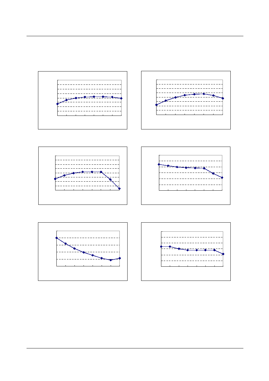
Typical Performance Characteristics
(These characteristic graphs are normalized at Ta=25
∞
C)
Fig.1 Operating Frequency
0.8
0.85
0.9
0.95
1
1.05
1.1
1.15
1.2
-25
0
25
50
75
100 125 150
Fosc
Fig.2 Feedback Source Current
0.8
0.85
0.9
0.95
1
1.05
1.1
1.15
1.2
-25
0
25
50
75
100 125 150
Ifb
Fig.3 Operating Current
0.8
0.85
0.9
0.95
1
1.05
1.1
1.15
1.2
-25
0
25
50
75
100 125 150
Iop
Fig.4 Max Inductor Current
0.8
0.85
0.9
0.95
1
1.05
1.1
-25
0
25
50
75
100 125 150
Ipeak
Fig.5 Start up Current
0.5
0.7
0.9
1.1
1.3
1.5
-25
0
25
50
75
100 125 150
Istart
Fig.6 Start Threshold Voltage
0.85
0.9
0.95
1
1.05
1.1
1.15
-25
0
25
50
75 100 125 150
Vstart
Figure 1. Operating Frequency
Figure 2. Feedback Source Current
Figure 3. Operating Supply Current
Figure 4. Peak Current Limit
Figure 5. Start up Current
Figure 6. Start Threshold Voltage
Temperature [
∞
C]
Temperature [
∞
C]
Temperature [
∞
C]
Temperature [
∞
C]
Temperature [
∞
C]
Temperature [
∞
C]
I
over