Document Outline
- Main Menu
- Analog & Mixed Signal
- SPS PSG
- SPS Index
- Search
- fairchildsemi.com

KA5Q0765RT
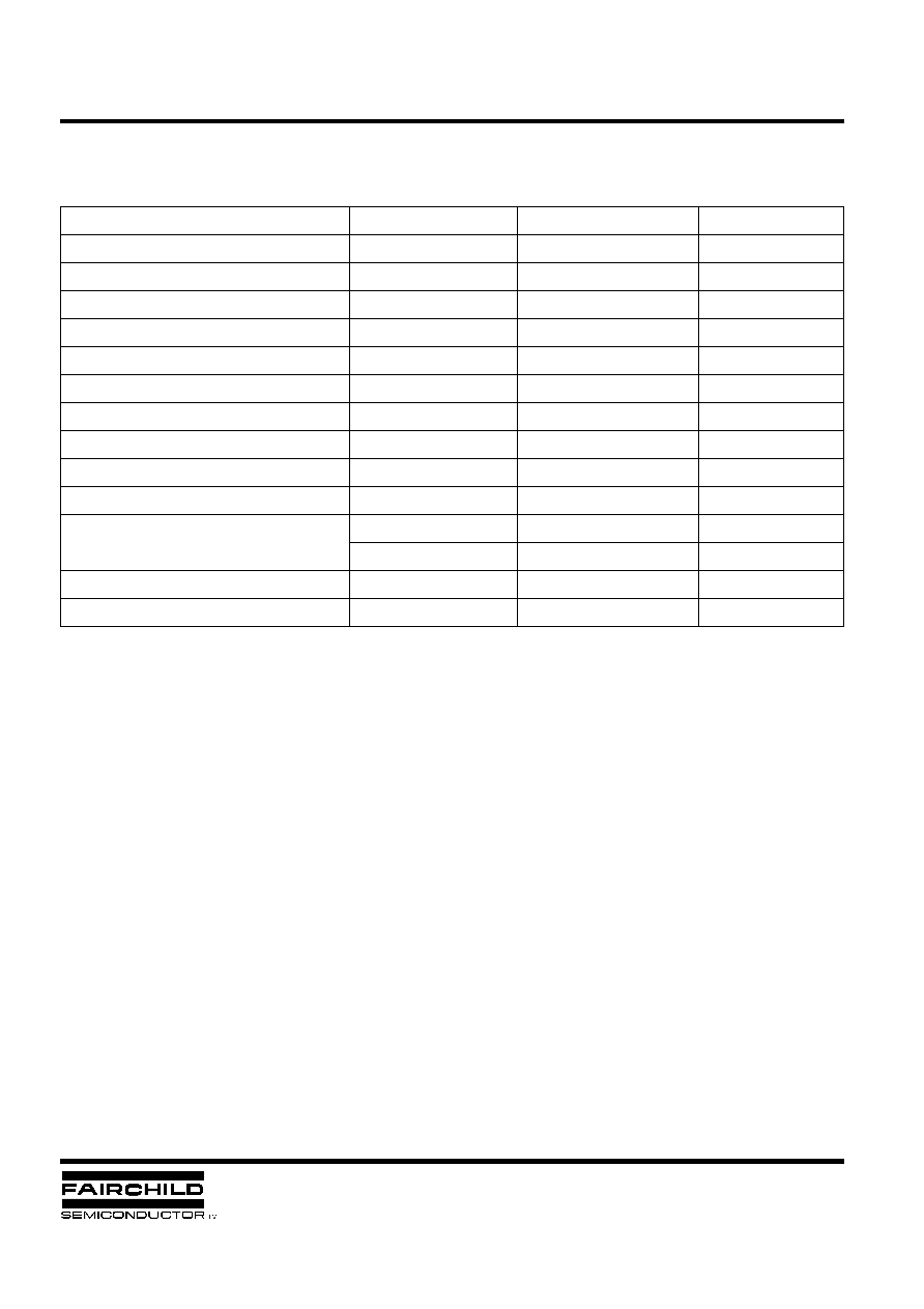
S P S
≠
+
≠
+
OSC
OVP
≠
+
LEB
≠
+
S _
Q
R
Delay
500nS
Vref
Internal
Bias
≠
+
≠
+
TSD
150
o
C
Power-on
Reset
S
Q
R
Burst mode
controller
Ifb
Ids
R
1.7R
Vds
REF.
PSR
REF.
Sync.
REF.
Ron
Roff
Rsense
Vfb offset
OCL
REF.
PWM
UVLO
Vz
5
4
3
1
2
S P S
FEATURES
∑
Quasi Resonant Converter Controller
∑
Internal Burst mode Controller for Stand-by mode
∑
Pulse by pulse current limiting
∑
Over current Latch protection
∑
Over voltage protection (Vsync: Min. 11V)
∑
Internal thermal shutdown function
∑
Under voltage lockout
∑
Internal high voltage sense FET
∑
Auto-restart mode
ORDERING INFORMATION
Device
Package
Topr (
∞
∞
∞
∞
C)
KA5Q0765RT
TO-220F-5L
-
25
∞
C to +85
∞
C
TO -22 0F -5L
1. Drain 2. GND 3. V
CC
4. FB 5. Sync
BLOCK DIAGRAM
The SPS product family is specially designed for an off-line SMPS
with minimal external components. The SPS consist of high voltage
power SenseFET and current mode PWM IC.
Included PWM controller features integrated fixed oscillator, under
voltage lock out, leading edge blanking, optimized gate turn-on/turn-
off driver, thermal shut down protection, over voltage protection, and
temperature compensated precision current sources for loop
compensation and fault protection circuitry. Compared to discrete
MOSFET and controller or RCC switching converter solution, a SPS
can reduce total component count, design size, and weight and at
the same time increase efficiency, productivity, and system reliability.
It has a basic platform well suited for cost-effective design in Quasi-
Resonant Converter as C-TV power supply.
1999 Fairchild Semiconductor Corporation
REV. B
KA5Q0765RT
S P S
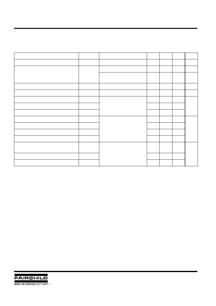
ABSOLUTE MAXIMUM RATINGS
NOTES:
1.
Tj=25
∞
C to 150
∞
C
2.
Repetitive rating: Pulse width limited by maximum junction temperature
3.
L=24mH, starting Tj=25
∞
C
4.
L=13uH, starting Tj=25
∞
C
Characteristic
Symbol
Value
Unit
Drain-source (GND) voltage
(1)
V
DSS
650
V
Drain-Gate voltage (R
GS
=1M
)
V
DGR
650
V
Gate-source (GND) voltage
V
GS
±
30
V
Drain current pulsed
(2)
I
DM
28.0
A
DC
Single pulsed avalanche energy
(3)
E
AS
570
mJ
Avalanche current
(4)
I
AS
20
A
Continuous drain current (T
C
=25
∞
C)
I
D
7.0
A
DC
Continuous drain current (T
C
=100
∞
C)
I
D
5.6
A
DC
Supply voltage
V
CC
30
V
Analog input voltage range
V
FB
-
0.3 to V
SD
V
Total power dissipation
P
D
(wt H/S)
135
W
Derating
1.1
W/
∞
C
Operating temperature
T
OPR
-
25 to +85
∞
C
Storage temperature
T
STG
-
55 to +150
∞
C
KA5Q0765RT
S P S
NOTE: Pulse test: Pulse width
300
µ
S, duty cycle
2%
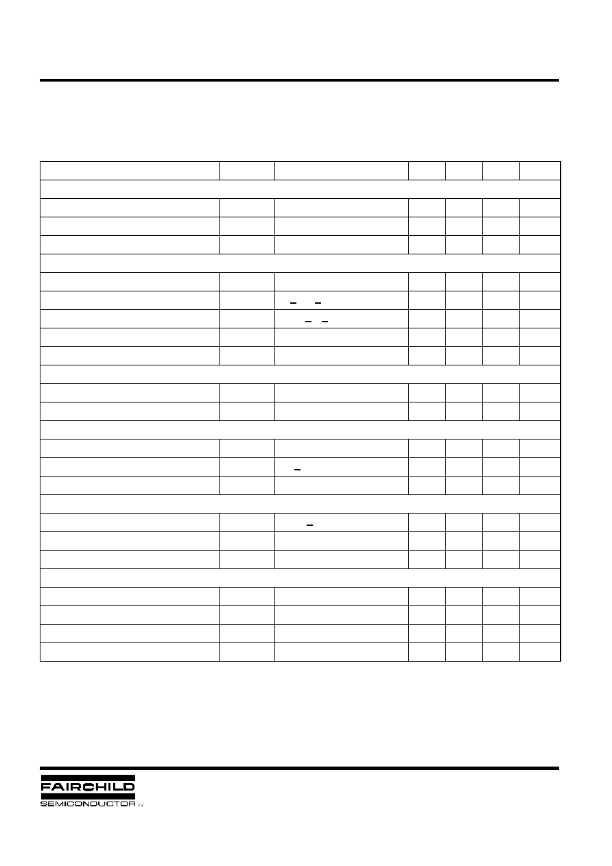
ELECTRICAL CHARACTERISTICS (SFET part)
(Ta=25
∞
C unless otherwise specified)
Characteristic
Symbol
Test condition
Min.
Typ.
Max.
Unit
Drain-source breakdown voltage
BV
DSS
V
GS
=0V, I
D
=50
µ
A
650
-
-
V
Zero gate voltage drain current
I
DSS
V
DS
=Max., Rating, V
GS
=0V
-
-
200
µ
A
V
DS
=0.8Max., Rating,
V
GS
=0V, T
C
=125
∞
C
-
-
500
µ
A
Static drain-source on resistance
(note)
R
DS(ON)
V
GS
=10V, I
D
=4.0A
-
1.25
1.6
Forward transconductance
(note)
gfs
V
DS
=15V, I
D
=4.0A
3.0
-
-
S
Input capacitance
Ciss
V
GS
=0V, V
DS
=25V,
f=1MHz
-
1600
-
pF
Output capacitance
Coss
-
310
-
Reverse transfer capacitance
Crss
-
120
-
Turn on delay time
td(on)
V
DD
=0.5BV
DSS
, I
D
=7.0A
(MOSFET switching
time are essentially
independent of
operating temperature)
-
25
-
nS
Rise time
tr
-
55
-
Turn off delay time
td(off)
-
80
-
Fall time
tf
-
50
-
Total gate charge
(gate-source+gate-drain)
Qg
V
GS
=10V, I
D
=7.0A,
V
DS
=0.5BV
DSS
(MOSFET
switching time are
essentially independent of
operating temperature)
-
-
72
nC
Gate-source charge
Qgs
-
9.3
-
Gate-drain (Miller) charge
Qgd
-
29.3
-
KA5Q0765RT
S P S
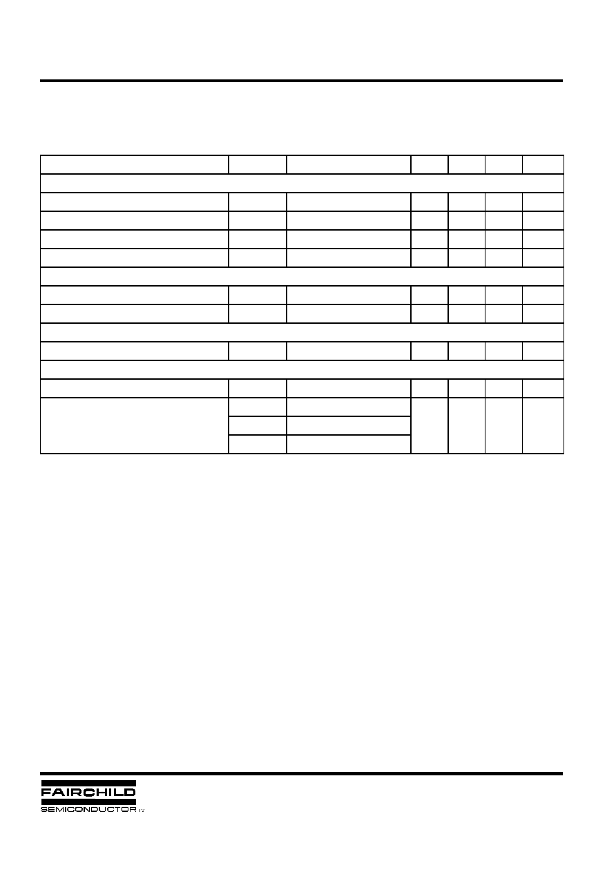
ELECTRICAL CHARACTERISTICS (Control part)
(Ta=25
∞
C unless otherwise specified)
Characteristic
Symbol
Test condition
Min.
Typ.
Max.
Unit
SENSE FET SECTION
Drain to PKG Breakdown voltage
BVpkg
60Hz AC, Ta=25
∞
C
3500
-
-
V
Drain to Source Breakdown voltage
BVdss
Vdrain=650V, Ta=25
∞
C
650
-
-
V
Drain to Source Leakage current
Idss
Vdrain=650V, Ta=25
∞
C
-
-
200
µ
A
OSCILLATOR SECTION
Initial Frequency
F
OSC
-
18
20
22
KHz
Voltage Stability
F
STABLE
12<V
CC
<23V
0
1
3
%
Temperature Stability
note 2
F
OSC
-25
∞
C<Ta<85
∞
C
0
±5
±10
%
Maximum Duty Cycle
D
MAX
-
92
95
98
%
Minimum Duty Cycle
D
MIN
-
-
-
0
%
UVLO SECTION
Start Threshold Voltage
V
START
V
FB
=GND
14
15
16
V
Stop Threshold Voltage
VSTOP
V
FB
=GND
8
9
10
V
FEEDBACK SECTION
Feedback Source Current
I
FB
V
FB
=GND
0.7
0.9
1.1
mA
Shotdown Feedback Voltage
V
SD
Vfb>6.9V
6.9
7.5
8.1
V
Shutdown Delay Current
I
DELAY
V
FB
=5V
4
5
6
µ
A
PROTECTION SECTION
Over Current Protection
V
OVP
Vsync>11V
11
12
13
V
Over Current Latch Voltage
note 2
V
OCL
-
0.9
1.0
1.1
V
Thermal shutdown Temp.
TSD
-
140
160
-
∞
C
SYNC SECTION
Normal Sync High Threshold Voltage
V
NSH
V
CC
=16V, Vfb=5V
4.0
4.6
5.2
V
Normal Sync Low Threshold Voltage
V
NSL
V
CC
=16V, Vfb=5V
2.3
2.6
2.9
V
Burst High Threshold Voltage
V
BSH
V
CC
=10.5V, Vfb=0V
3.2
3.6
4.0
V
Burst Low Threshold Voltage
V
BSL
V
CC
=10.5V, Vfb=0V
1.1
1.3
1.5
V
KA5Q0765RT
S P S
ELECTRICAL CHARACTERISTICS (Continued)
(Ta=25
∞
C unless otherwise specified)
NOTE:
1.
These parameters, although guaranteed, are not 100% tested in production
2.
These parameters, although guaranteed, are tested in EDS (wafer test) process
3.
These parameters indicate inductor current
Characteristic
Symbol
Test condition
Min.
Typ.
Max.
Unit
BURST MODE SECTION
Burst mode Low Threshold Voltage
V
BURL
Vfb=0V
10.4
11.0
11.6
V
Burst mode High Threshold Voltage
V
BURH
Vfb=0V
11.4
12.0
12.6
V
Burst mode Enable Feedback voltage
V
BEN
V
CC
=10.5V
0.7
1.0
1.3
V
Burst mode Peak Current Limit
I
BU_PK
V
CC
=10.5V
0.65
0.85
1.0
V
PRIMARY SIDE REGULATION SECTION
Primary Regulation Threshold Voltage
V
PR
Ifb=700
µ
A, Vfb=4V
32.0
32.5
33.0
V
Primary Regulation Thansconductance
G
PR
-
2.0
2.6
-
mA/V
CURRENT LIMIT (SELF-PROTECTION) SECTION
Peak Current Limit
note 3
I
PK
-
4.4
5.0
5.6
A
START UP CURRENT
Start up Current
I
START
Vfb=GND, V
CC
=14V
-
0.1
0.2
mA
Operatig Supply Current
noet 1
I
OP
Vfb=GND, V
CC
=16V
-
10
18
mA
I
OP(MIN)
Vfb=GND, V
CC
=12V
I
OP(MAX)
Vfb=GND, V
CC
=28V