
©2003 Fairchild Semiconductor Corporation
www.fairchildsemi.com
Rev.1.0.3
Features
∑ Quasi Resonant Converter Controller
∑ Internal Burst Mode Controller for Stand-by Mode
∑ Pulse by Pulse Current Limiting
∑ Over Current Latch Protection
∑ Over Voltage Protection (Vsync: Min. 11V)
∑ Internal Thermal Shutdown Function
∑ Under Voltage Lockout
∑ Internal High Voltage Sense FET
∑ Auto-Restart Mode
Description
The Fairchild Power Switch(FPS) product family is specially
designed for an off-line SMPS with minimal external
components. The Fairchild Power Switch(FPS) consist of high
voltage power SenseFET and current mode PWM controller IC.
PWM controller features integrated fixed oscillator, under
voltage lock out, leading edge blanking, optimized gate turn-on/
turn-off driver, thermal shut down protection, over voltage
protection, temperature compensated precision current sources
for loop compensation and fault protection circuit. compared to
discrete MOSFET and controller or R
CC
switching converter
solution, a Fairchild Power Switch(FPS) can reduce total
component count, design size, and weight and at the same time
increase & efficiency, productivity, and system reliability. It has
a basic platform well suited for cost-effective design in quasi
resonant converter as C-TV power supply.
TO-220F-5L
1. Drain 2. GND 3. V
CC
4. FB 5. Sync
TO-3PF-5L
1
1
Internal Block Diagram
-
+
Rsense
11V on
12V off
3
1
2
4
VREF
Internal
BIAS
S
Q
R
LEB
450ns
S
QB
R
Ro
n
Rof
f
Power
on
Reset
OVP
OLP
7.5V
-
+
12V
Sync
-
+
-
+
UVLO
15V/9V
5
Burst Mode
3.5V/1.25V
SYNC
SYNC
SYNC
SYNC
-
+
R
2.5R
-
+
-
+
Offset
Thermal
Thermal
Thermal
Thermal
Shut Down
Shut Down
Shut Down
Shut Down
S
Q
R
Power on Reset
(VCC=6.5V)
Delay
80ns
1V
-
+
OCL
1V
FEEDBACK
FEEDBACK
FEEDBACK
FEEDBACK
VCC
VCC
VCC
VCC
DRAIN
DRAIN
DRAIN
DRAIN
SOURCE
SOURCE
SOURCE
SOURCE
Normal Mode
4.6V/2.6V
OSC
-
+
-
+
Idelay
Ifb
VREF
32V 1%
+
-
Ron
Roff
KA5Q-SERIES
KA5Q0765RT/KA5Q12656RT/KA5Q1265RF/
KA5Q1565RF
Fairchild Power Switch(FPS)

KA5Q-SERIES
2
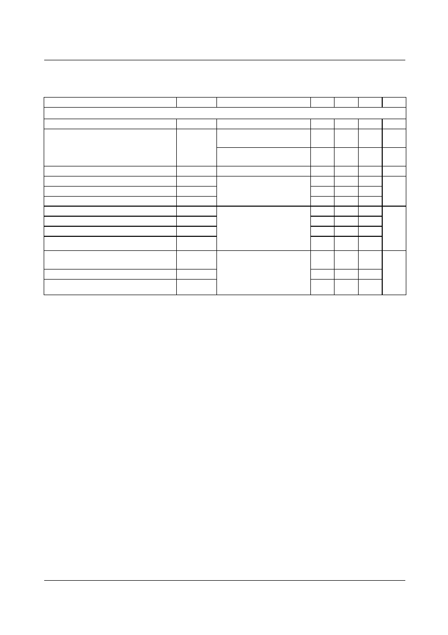
Absolute Maximum Ratings
(Ta=25
∞
C, unless otherwise specified)
Absolute Maximum Ratings
(Continued)
Characteristic
Symbol
Value
Unit
KA5Q0765RT
Drain-Gate Voltage(R
GS
=1M
)
V
DGR
650
V
Gate-Source(GND) Voltage
V
GS
±30
V
Drain Current Pulsed
(1)
I
DM
28
ADC
Continuous Drain Current (Tc = 25
∞
C)
I
D
7.0
ADC
Continuous Drain Current (Tc = 100
∞
C)
I
D
5.6
ADC
Single Pulsed Avalanch Current
(3)
(Energy
(2)
)
I
AS
(E
AS
)
20(570)
A(mJ)
Maximum Supply Voltage
V
CC,MAX
40
V
Input Voltage Range
V
FB
-0.3 to V
CC
V
V
Sync
-0.3 to 13
V
Total Power Dissipation
P
D
47
W
Derating
0.37
W/
∞
C
Operating Junction Temperature.
T
J
+160
∞
C
Operating Ambient Temperature.
T
A
-25 to +85
∞
C
Storage Temperature Range.
T
STG
-55 to +150
∞
C
Thermal Resistance
Rthjc
2.7
∞
C/W
KA5Q12656RT
Drain-Gate Voltage(R
GS
=1M
)
V
DGR
650
V
Gate-Source(GND) Voltage
V
GS
±30
V
Drain Current Pulsed
(1)
I
DM
48
ADC
Continuous Drain Current (Tc = 25
∞
C)
I
D
12
ADC
Continuous Drain Current (Tc = 100
∞
C)
I
D
8.4
ADC
Single Pulsed Avalanch Current(Energy
(2)
)
I
AS
(E
AS
)
30(950)
A(mJ)
Maximum Supply Voltage
V
CC,MAX
40
V
Input Voltage Range
V
FB
-0.3 to V
CC
V
V
Sync
-0.3 to13
V
Total Power Dissipation
P
D
55
W
Derating
0.4
W/
∞
C
Operating Junction Temperature.
T
J
+160
∞
C
Operating Ambient Temperature.
T
A
-25 to +85
∞
C
Storage Temperature Range.
T
STG
-55 to +150
∞
C
Thermal Resistance
Rthjc
2.5
∞
C/W

KA5Q-SERIES
3
(Ta=25
∞
C, unless otherwise specified)
Note:
1. Repetitive rating : Pulse width limited by maximum junction temperature
2. L = 10mH, V
DD
=50V, R
G
= 27
, starting Tj = 25
∞
C
3. L = 13uH, starting Tj = 25
∞
C
Characteristic
Symbol
Value
Unit
KA5Q1265RF
Drain-Gate Voltage(R
GS
=1M
)
V
DGR
650
V
Gate-Source(GND) Voltage
V
GS
±30
V
Drain Current Pulsed
(1)
I
DM
48
ADC
Continuous Drain Current (Tc = 25
∞
C)
I
D
12
ADC
Continuous Drain Current (Tc = 100
∞
C)
I
D
8.4
ADC
Single Pulsed Avalanch Current(Energy
(2)
)
I
AS
(E
AS
)
33(950)
A(mJ)
Maximum Supply Voltage
V
CC,MAX
40
V
Input Voltage Range
V
FB
-0.3 to V
CC
V
V
Sync
-0.3 to 13
V
Total Power Dissipation
P
D
95
W
Derating
0.76
W/
∞
C
Operating Junction Temperature.
T
J
+160
∞
C
Operating Ambient Temperature.
T
A
-25 to +85
∞
C
Storage Temperature Range.
T
STG
-55 to +150
∞
C
Thermal Resistance
Rthjc
1.31
∞
C/W
KA5Q1565RF
Drain-Gate Voltage(R
GS
=1M
)
V
DGR
650
V
Gate-Source(GND) Voltage
V
GS
±30
V
Drain Current Pulsed
(1)
I
DM
60
ADC
Continuous Drain Current (Tc = 25
∞
C)
I
D
15
ADC
Continuous Drain Current (Tc = 100
∞
C)
I
D
12.0
ADC
Single Pulsed Avalanch Current(Energy
(2)
)
I
AS
(E
AS
)
36(1050)
A(mJ)
Maximum Supply Voltage
V
CC,MAX
40
V
Input Voltage Range
V
FB
-0.3 to V
CC
V
V
Sync
-0.3 to 13
V
Total Power Dissipation
P
D
98
W
Derating
0.78
W/
∞
C
Operating Junction Temperature.
T
J
+160
∞
C
Operating Ambient Temperature.
T
A
-25 to +85
∞
C
Storage Temperature Range.
T
STG
-55 to +150
∞
C
Thermal Resistance
Rthjc
1.28
∞
C/W

KA5Q-SERIES
4
Electrical Characteristics (SFET part)
(Ta=25
∞
C unless otherwise specified)
Parameter
Symbol
Conditions
Min.
Typ.
Max.
Unit
KA5Q0765RT
Drain-Source Breakdown Voltage
BV
DSS
V
GS
=0V, I
D
=50
µ
A
650
-
-
V
Zero Gate Voltage Drain Current
I
DSS
V
DS
=Max., Rating, V
GS
=0V
-
-
200
µ
A
V
DS
=0.8Max., Rating,
V
GS
=0V, T
C
=85
∞
C
-
-
300
µ
A
Static Drain-Source on Resistance
(1)
R
DS
(on)
V
GS
=10V, I
D
=4.0A
-
1.3
1.6
Input Capacitance
Ciss
V
GS
=0V, V
DS
=25V,
f = 1MHz
-
1110
-
pF
Output Capacitance
Coss
-
105
-
Reverse Transfer Capacitance
Crss
-
50
-
Turn on Delay Time
td(on)
V
DD
=0.5BV
DSS
, I
D
=7.0A
(MOSFET switching
time are essentially
independent of
operating temperature)
-
25
-
nS
Rise Time
tr
-
55
-
Turn Off Delay Time
td(off)
-
80
-
Fall Time
tf
-
50
-
Total Gate Charge
(Gate-Source+Gate-Drain)
Qg
V
GS
=10V, I
D
=7.0A,
V
DS
=0.5BV
DSS
(MOSFET
Switching time are
Essentially independent of
Operating temperature)
-
57
74
nC
Gate-Source Charge
Qgs
-
9.3
-
Gate-Drain (Miller) Charge
Qgd
-
29.3
-
KA5Q12656RT/KA5Q1265RF
Drain-Source Breakdown Voltage
BV
DSS
V
GS
=0V, I
D
=50
µ
A
650
-
-
V
Zero Gate Voltage Drain Current
I
DSS
V
DS
=Max., Rating, V
GS
=0V
-
-
200
µ
A
V
DS
=0.8Max., Rating,
V
GS
=0V, T
C
=85
∞
C
-
-
300
µ
A
Static Drain-Source on Resistance
(1)
R
DS(on)
V
GS
=10V, I
D
=6A
-
0.7
0.9
Input Capacitance
Ciss
V
GS
=0V, V
DS
=25V,
f = 1MHz
-
1820
-
pF
Output Capacitance
Coss
-
185
-
Reverse Transfer Capacitance
Crss
-
32
-
Turn on Delay Time
td(on)
V
DD
=0.5BV
DSS
, I
D
=12.0A
(MOSFET switching
time are essentially
independent of
operating temperature)
-
38
-
nS
Rise Time
tr
-
120
-
Turn Off Delay Time
td(off)
-
200
-
Fall Time
tf
-
100
-
Total Gate Charge
(Gate-Source+Gate-Drain)
Qg
V
GS
=10V, I
D
=12.0A,
V
DS
=0.5BV
DSS
(MOSFET
Switching time are
Essentially independent of
Operating temperature)
-
60
78
nC
Gate-Source Charge
Qgs
-
10
-
Gate-Drain (Miller) Charge
Qgd
-
30
-
KA5Q-SERIES
5
Absolute Maximum Ratings (SFET Part)
(Ta=25
∞
C, unless otherwise specified)
Note:
1. Pulse test: Pulse width
300
µ
S, duty cycle
2%
Characteristic
Symbol
Test condition
Min.
Typ.
Max.
Unit
KA5Q1565RF
Drain-Source Breakdown Voltage
BV
DSS
V
GS
=0V, I
D
=50
µ
A
650
-
-
V
Zero Gate Voltage Drain Current
I
DSS
V
DS
=Max., Rating,
V
GS
=0V
-
-
200
µ
A
V
DS
=0.8Max., Rating,
V
GS
=0V, T
C
=85
∞
C
-
-
300
µ
A
Static Drain-Source on Resistance
(Note)
R
DS(ON)
V
GS
=10V, I
D
=7.3A
-
0.5
0.65
W
Input Capacitance
Ciss
V
GS
=0V, V
DS
=25V,
f=1MHz
-
2580
-
pF
Output Capacitance
Coss
-
270
-
Reverse Transfer Capacitance
Crss
-
50
-
Turn on Delay Time
td(on)
V
DD
=0.5BV
DSS
, I
D
=14.6A
(MOSFET switching
time are essentially
independent of
operating temperature)
-
50
-
nS
Rise Time
tr
-
155
-
Turn Off Delay Time
td(off)
-
270
-
Fall Time
tf
-
125
-
Total Gate Charge
(Gate-Source+Gate-Drain)
Qg
V
GS
=10V, I
D
=14.6A,
V
DS
=0.8BV
DSS
(MOSFET
switching time are
essentially independent of
operating temperature)
-
90
117
nC
Gate-Source Charge
Qgs
-
15
-
Gate-Drain (Miller) Charge
Qgd
-
45
-