 | –≠–ª–µ–∫—Ç—Ä–æ–Ω–Ω—ã–π –∫–æ–º–ø–æ–Ω–µ–Ω—Ç: KA7500BD | –°–∫–∞—á–∞—Ç—å:  PDF PDF  ZIP ZIP |
©2002 Fairchild Semiconductor Corporation
www.fairchildsemi.com
Rev. 1.0.0
Features
∑ Internal Regulator Provides a Stable 5V Reference Supply
Trimmed to 5%
∑ Uncommitted Output TR for 200mA Sink or Source
Current
∑ Output Control For Push-Pull or Single Ended Operation
∑ Variable Duty Cycle By Dead Time Control (Pin 4)
Complete PWM Control Circuit
∑ On-Chip Oscillator With Master or Slave Operation
∑ Internal Circuit Prohibits Double Pulse at Either Output
Description
The KA7500B is used for the control circuit of the PWM
switching regulator. The KA7500B consists of 5V reference
voltage circuit, two error amplifiers, a flip flop, an output
control circuit, a PWM comparator, a dead time comparator
and an oscillator. This device can be operated in the
switching frequency of 1kHz to 300kHz.
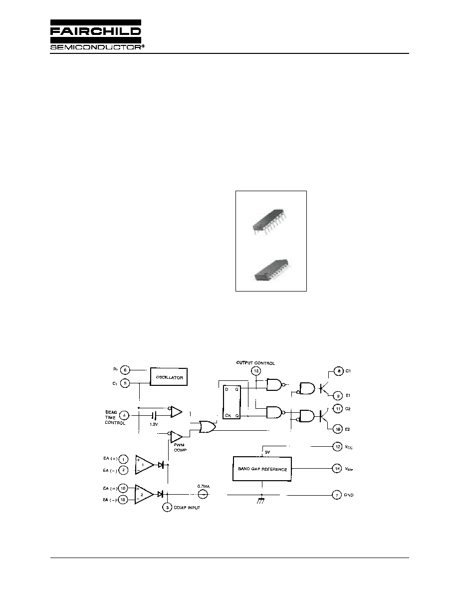
16-DIP
16-SOP
1
1
Internal Block Diagram
KA7500B
SMPS Controller
KA7500B
2
Absolute Maximum Ratings
Parameter
Symbol
Value
Unit
Supply Voltage
V
CC
42
V
Collector Supply Voltage
V
C
42
V
Output Current
I
O
250
mA
Amplifier Input Voltage
V
IN
V
CC
+0.3
V
Power Dissipation (T
A
= 25
∞
C)
P
D
1 (KA7500B)
0.9 (KA7500BD)
W
Operating Temperature Range
T
OPR
0 ~ +70
∞
C
Storage Temperature Range
T
STG
-65 ~ +150
∞
C
KA7500B
3
Electrical Characteristics
(V
CC
= 20V, f = 10kHz, T
A
= 0
∞
C to +70
∞
C, unless otherwise specified)
Note:
1. This parameter, although guaranteed, is not 100% tested in production.
Parameter
Symbol
Conditions
Min.
Typ.
Max.
Unit
REFERENCE SECTION
Reference Output Voltage
V
REF
I
REF
= 1mA
4.75
5.0
5.25
V
Line Regulation
V
REF
V
CC
= 7V to 40V
-
2.0
25
mV
Temperature Coefficient of V
REF
V
REF
/
T
T
A
= 0
∞
C to 70
∞
C
-
0.01
0.03
%/
∞
C
Load Regulation
V
REF
I
REF
= 1mA to 10mA
-
1.0
15
mV
Short-Circuit Output Current
I
SC
V
REF
= 0V
10
35
50
mA
OSCILLATOR SECTION
Oscillation Frequency
f
C
T
= 0.01
µ
F, R
T
= 12k
-
10
-
kHz
Frequency Change with Temperature
f/
T
C
T
= 0.01
µ
F, R
T
= 12k
-
-
2
%
DEAD TIME CONTROL SECTION
Input Bias Current
I
BIAS
V
CC
= 15V, 0V
V
4
5.25V
-
-2.0
-10
µ
A
Maximum Duty Cycle
D
(MAX)
V
CC
= 15V, V
4
= 0V
O.C Pin = V
REF
45
-
-
%
Input Threshold Voltage
V
ITH
Zero Duty Cycle
-
3.0
3.3
V
Max. Duty Cycle
0
-
-
ERROR AMP SECTION
Input Offset Voltage
V
IO
V
3
= 2.5V
-
2.0
10
mV
Input Offset Current
I
IO
V
3
= 2.5V
-
25
250
mA
Input Bias Current
I
BIAS
V
3
= 2.5V
-
0.2
1.0
µ
A
Common Mode Input Voltage
V
CM
7V
V
CC
40V
-0.3
-
V
CC
V
Open-Loop Voltage Gain
G
VO
0.5V
V
3
3 .5V
70
95
-
dB
Unit-Gain Bandwidth (Note1)
BW
-
-
650
-
kHz
PWM COMPARATOR SECTION
Input Threshold Voltage
V
ITH
Zero Duty Cycle
-
4
4.5
V
Input Sink Current
I
SINK
V
3
=0.7V
-0.3
-0.7
-
mV
OUTPUT SECTION
Output Saturation Voltage
Common Emitter
V
CE(SAT)
V
E
= 0, I
C
= 200mA
-
1.1
1.3
V
Common Collector
V
CC(SAT)
V
C
= 15V, I
E
= -200mA
-
1.5
2.5
Collector Off-State Current
I
C(OFF)
V
CC
= 40V, V
CE
= 40V
-
2
100
µ
A
Emitter Off-State Current
I
E(OFF)
V
CC
= V
C
= 40V, V
E
= 0
-
-
-100
TOTAL DEVICE
Supply Current
I
CC
Pin 6 = V
REF
, V
CC
= 15V
-
6
10
mA
OUTPUT SWITCHING CHARACTERISTICS
Rise Time
t
R
-
-
-
-
-
Common Emitter
-
-
-
100
200
ns
Common Collector
-
-
-
100
200
Fall Time
t
F
-
-
-
-
-
Common Emitter
-
-
-
25
100
ns
Common Collector
-
-
-
40
100
KA7500B
4
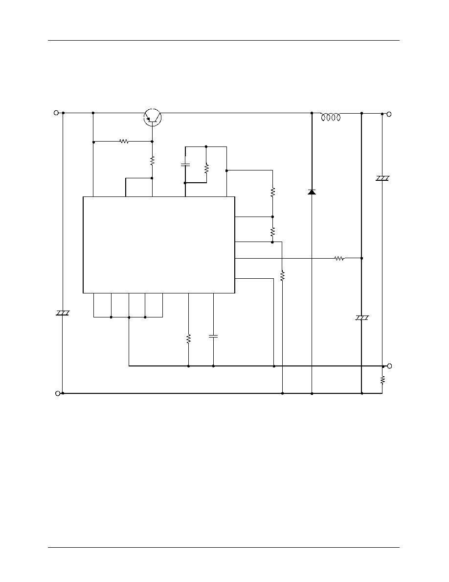
Typical Application
Pulse Width Modulated Step-down Converter
KA7500B
12
Vcc
11
C2
8
C1
3
COMP INPUT
- 2
V
REF
14
- 15
+ 1
+16
D.T
4
GND
7
E1
9
E2
10
O.C
13
R
T
6
C
T
5
KSA1010
1mH,2A
Vo=5V
Io=1A
V
I
=10V to 40V
47
150
1M
0.1uF
50uF
10V
5.1k
50uF
10V
GND
0.1
0.001uF
50uF
50V
5.1k
150
47k
5.1k
+
+
+
KA7500B
5
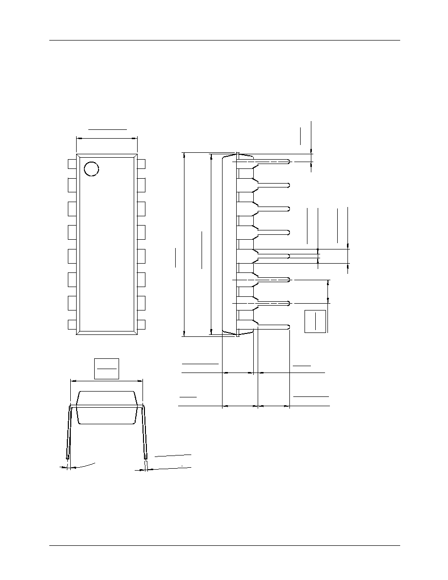
Mechanical Dimensions
Package
#1
#8
#9
#16
6.40
±
0.20
7.62
0.300
2.54
0.100
0.252
±
0.008
0~15
∞
0.25
+0.10
≠0.05
0.010
+0.004
≠0.002
3.30
±
0.30
0.130
±
0.012
3.25
±
0.20
0.128
±
0.008
19.40
±
0.20
0.764
±
0.008
19.80
0.780
MAX
5.08
0.200
0.38
0.014
MAX
MIN
0.81
0.032
()
0.46
±
0.10
0.018
±
0.004
0.059
±
0.004
1.50
±
0.10
16-DIP
KA7500B
6
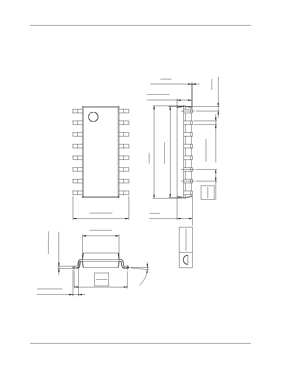
Mechanical Dimensions
(Continued)
Package
0.70
±
0.20
0.0275
±
0.008
#1
#8
#9
#16
9.90
±
0.20
0.39
±
0.008
1.27
0.050
5.72
0.225
1.55
±
0.10
0.061
±
0.004
0.05
0.002
6.00
±
0.30
0.236
±
0.012
3.95
±
0.20
0.156
±
0.008
10.30
0.405
MAX
0~8
∞
0.51
0.020
()
1.80
0.071
MAX0.10
MAX0.004
MAX
MIN
+
0.10
-0.05
0.20
+
0.004
-0.002
0.008
+
0.10
-0.05
0.406
+
0.004
-0.002
0.016
16-SOP
KA7500B
7
Ordering Information
Product Number
Package
Operating Temperature
KA7500B
16-DIP
0 ~ +70
∞
C
KA7500BD
16-SOP

KA7500B
9/10/02 0.0m 001
Stock#DSxxxxxxxx
2002 Fairchild Semiconductor Corporation
LIFE SUPPORT POLICY
FAIRCHILD'S PRODUCTS ARE NOT AUTHORIZED FOR USE AS CRITICAL COMPONENTS IN LIFE SUPPORT DEVICES
OR SYSTEMS WITHOUT THE EXPRESS WRITTEN APPROVAL OF THE PRESIDENT OF FAIRCHILD SEMICONDUCTOR
CORPORATION. As used herein:
1. Life support devices or systems are devices or systems
which, (a) are intended for surgical implant into the body,
or (b) support or sustain life, and (c) whose failure to
perform when properly used in accordance with
instructions for use provided in the labeling, can be
reasonably expected to result in a significant injury of the
user.
2. A critical component in any component of a life support
device or system whose failure to perform can be
reasonably expected to cause the failure of the life support
device or system, or to affect its safety or effectiveness.
www.fairchildsemi.com
DISCLAIMER
FAIRCHILD SEMICONDUCTOR RESERVES THE RIGHT TO MAKE CHANGES WITHOUT FURTHER NOTICE TO ANY
PRODUCTS HEREIN TO IMPROVE RELIABILITY, FUNCTION OR DESIGN. FAIRCHILD DOES NOT ASSUME ANY
LIABILITY ARISING OUT OF THE APPLICATION OR USE OF ANY PRODUCT OR CIRCUIT DESCRIBED HEREIN; NEITHER
DOES IT CONVEY ANY LICENSE UNDER ITS PATENT RIGHTS, NOR THE RIGHTS OF OTHERS.