 | –≠–ª–µ–∫—Ç—Ä–æ–Ω–Ω—ã–π –∫–æ–º–ø–æ–Ω–µ–Ω—Ç: KA7805ETU | –°–∫–∞—á–∞—Ç—å:  PDF PDF  ZIP ZIP |
©2003 Fairchild Semiconductor Corporation
www.fairchildsemi.com
Rev. 1.0.0
Features
∑ Output Current up to 1A
∑ Output Voltages of 5, 6, 8, 9, 12, 15, 18, 24V
∑ Thermal Overload Protection
∑ Short Circuit Protection
∑ Output Transistor Safe Operating Area Protection
Description
The KA78XXE/KA78XXAE series of three-terminal posi-
tive regulator are available in the TO-220/D-PAK package
and with several fixed output voltages, making them useful
in a wide range of applications. Each type employs internal
current limiting, thermal shut down and safe operating area
protection, making it essentially indestructible. If adequate
heat sinking is provided, they can deliver over 1A output
current. Although designed primarily as fixed voltage
regulators, these devices can be used with external
components to obtain adjustable voltages and currents.
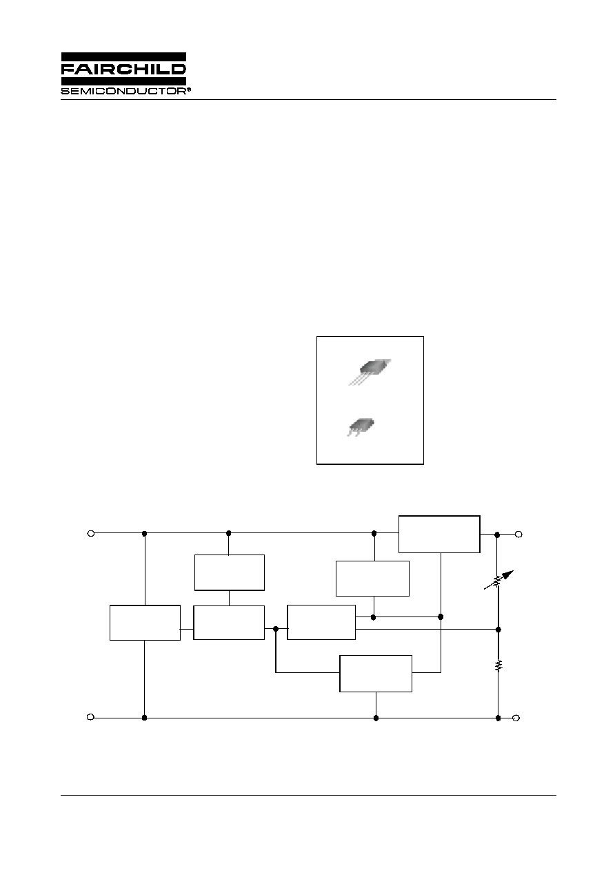
TO-220
D-PAK
1. Input 2. GND 3. Output
1
1
GND
GND
Internal Block Diagram
SERIES
PASS
ELEMENT
SOA
PROTECTION
ERROR
AMPLIFIER
THERMAL
PROTECTION
CURRENT
GENERATOR
REFERENCE
VOLTAGE
STARTING
CIRCUIT
OUTPUT
3
GND
2
INPUT
1
KA78XXE/KA78XXAE
3-Terminal 1A Positive Voltage Regulator
KA78XXE/KA78XXAE
2
Absolute Maximum Ratings
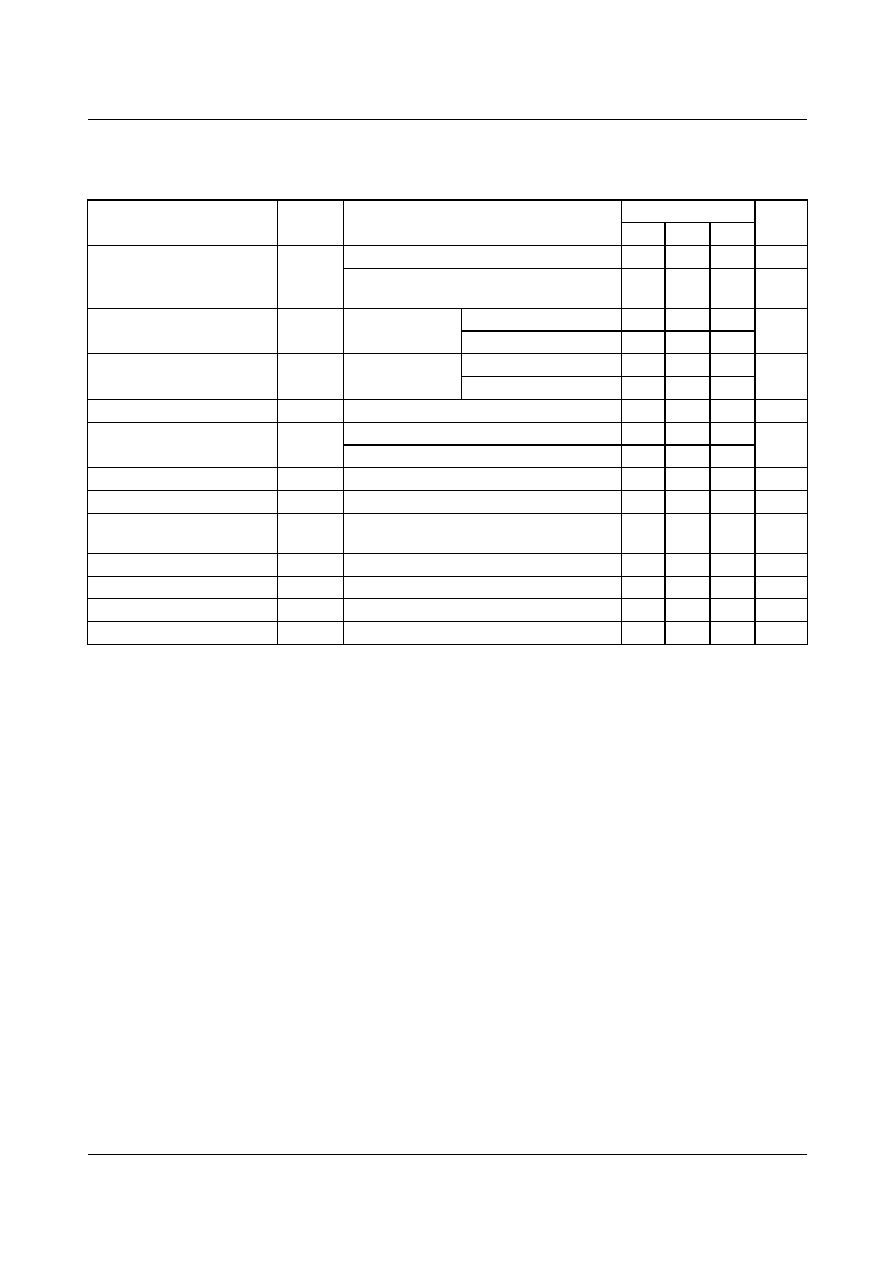
Electrical Characteristics (KA7805E/KA7805ER)
(Refer to test circuit, 0
∞
C < T
J
< 125
∞
C, I
O
= 500mA, V
I
=10V, C
I
= 0.33
µ
F, C
O
=0.1
µ
F, unless otherwise specified)
Note:
1. Load and line regulation are specified at constant junction temperature. Changes in V
o
due to heating effects must be taken
into account separately. Pulse testing with low duty is used.
2. These parameters, although guaranteed, are not 100% tested in production.
Parameter
Symbol
Value
Unit
Input Voltage (for V
O
= 5V to 18V)
(for V
O
= 24V)
V
I
V
I
35
40
V
V
Thermal Resistance Junction-Cases (TO-220)
R
JC
5
∞
C/W
Thermal Resistance Junction-Air (TO-220)
R
JA
65
∞
C/W
Operating Temperature Range (KA78XXE/AE/ER)
T
OPR
0 ~ +125
∞
C
Storage Temperature Range
T
STG
-65 ~ +150
∞
C
Parameter
Symbol
Conditions
KA7805E
Unit
Min.
Typ. Max.
Output Voltage
V
O
T
J
=+25
∞
C
4.8
5.0
5.2
5.0mA
Io
1.0A, P
O
15W
V
I
= 7V to 20V
4.75
5.0
5.25
V
Line Regulation (Note1)
Regline
T
J
=+25
∞
C
V
O
= 7V to 25V
-
4.0
100
mV
V
I
= 8V to 12V
-
1.6
50
Load Regulation (Note1)
Regload
T
J
=+25
∞
C
I
O
= 5.0mA to1.5A
-
9
100
mV
I
O
=250mA to 750mA
-
4
50
Quiescent Current
I
Q
T
J
=+25
∞
C
-
5.0
8.0
mA
Quiescent Current Change
I
Q
I
O
= 5mA to 1.0A
-
0.03
0.5
mA
V
I
= 7V to 25V
-
0.3
1.3
Output Voltage Drift (Note2)
V
O
/
T
I
O
= 5mA
-
-0.8
-
mV/
∞
C
Output Noise Voltage
V
N
f = 10Hz to 100kHz, T
A
=+25
∞
C
-
42
-
µ
V/V
O
Ripple
Rejection (Note2)
RR
f = 120Hz
V
O
= 8V to 18V
62
73
-
dB
Dropout Voltage
V
Drop
I
O
= 1A, T
J
=+25
∞
C
-
2
-
V
Output Resistance (Note2)
r
O
f = 1kHz
-
15
-
m
Short Circuit Current
I
SC
V
I
= 35V, T
A
=+25
∞
C
-
230
-
mA
Peak Current (Note2)
I
PK
T
J
=+25
∞
C
-
2.2
-
A
KA78XXE/KA78XXAE
3
Electrical Characteristics (KA7806E/KA7806ER)
(Continued)
(Refer to test circuit, 0
∞
C < T
J
< 125
∞
C, I
O
= 500mA, V
I
=11V, C
I
= 0.33
µ
F, C
O
=0.1
µ
F, unless otherwise specified)
Note:
1. Load and line regulation are specified at constant junction temperature. Changes in V
O
due to heating effects must be taken
into account separately. Pulse testing with low duty is used.
2. These parameters, although guaranteed, are not 100% tested in production.
Parameter
Symbol
Conditions
KA7806E
Unit
Min. Typ. Max.
Output Voltage
V
O
T
J
=+25
∞
C
5.75
6.0
6.25
5.0mA
I
O
1.0A, P
O
15W
V
I
= 8.0V to 21V
5.7
6.0
6.3
V
Line Regulation (Note1)
Regline
T
J
=+25
∞
C
V
I
= 8V to 25V
-
5
120
mV
V
I
= 9V to 13V
-
1.5
60
Load Regulation (Note1)
Regload
T
J
=+25
∞
C
I
O
=5mA to 1.5A
-
9
120
mV
I
O
=250mA to 750mA
-
3
60
Quiescent Current
I
Q
T
J
=+25
∞
C
-
5.0
8.0
mA
Quiescent Current Change
I
Q
I
O
= 5mA to 1A
-
-
0.5
mA
V
I
= 8V to 25V
-
-
1.3
Output Voltage Drift (Note2)
V
O
/
T
I
O
= 5mA
-
-0.8
-
mV/
∞
C
Output Noise Voltage
V
N
f = 10Hz to 100kHz, T
A
=+25
∞
C
-
45
-
µ
V/Vo
Ripple
Rejection (Note2)
RR
f = 120Hz
V
I
= 9V to 19V
59
75
-
dB
Dropout Voltage
V
Drop
I
O
= 1A, T
J
=+25
∞
C
-
2
-
V
Output Resistance(Note2)
r
O
f = 1kHz
-
19
-
m
Short Circuit Current
I
SC
V
I
= 35V, T
A
=+25
∞
C
-
250
-
mA
Peak Current (Note2)
I
PK
T
J
=+25
∞
C
-
2.2
-
A
KA78XXE/KA78XXAE
4
Electrical Characteristics (KA7808E/KA7808ER)
(Continued)
(Refer to test circuit, 0
∞
C < T
J
< 125
∞
C, I
O
= 500mA, V
I
=14V, C
I
= 0.33
µ
F, C
O
=0.1
µ
F, unless otherwise specified)
Note:
1. Load and line regulation are specified at constant junction temperature. Changes in V
O
due to heating effects must be taken
into account separately. Pulse testing with low duty is used.
2. These parameters, although guaranteed, are not 100% tested in production.
Parameter
Symbol
Conditions
KA7808E
Unit
Min.
Typ. Max.
Output Voltage
V
O
T
J
=+25
∞
C
7.7
8.0
8.3
5.0mA
I
O
1.0A, P
O
15W
V
I
= 10.5V to 23V
7.6
8.0
8.4
V
Line Regulation (Note1)
Regline
T
J
=+25
∞
C
V
I
= 10.5V to 25V
-
5.0
160
mV
V
I
= 11.5V to 17V
-
2.0
80
Load Regulation (Note1)
Regload
T
J
=+25
∞
C
I
O
= 5.0mA to 1.5A
-
10
160
mV
I
O
= 250mA to 750mA
-
5.0
80
Quiescent Current
I
Q
T
J
=+25
∞
C
-
5.0
8.0
mA
Quiescent Current Change
I
Q
I
O
= 5mA to 1.0A
-
0.05
0.5
mA
V
I
= 10.5A to 25V
-
0.5
1.0
Output Voltage Drift (Note2)
V
O
/
T
I
O
= 5mA
-
-0.8
-
mV/
∞
C
Output Noise Voltage
V
N
f = 10Hz to 100kHz, T
A
=+25
∞
C
-
52
-
µ
V/Vo
Ripple
Rejection (Note2)
RR
f = 120Hz, V
I
= 11.5V to 21.5V
56
73
-
dB
Dropout Voltage
V
Drop
I
O
= 1A, T
J
=+25
∞
C
-
2
-
V
Output Resistance (Note2)
r
O
f = 1kHz
-
17
-
m
Short Circuit Current
I
SC
V
I
= 35V, T
A
=+25
∞
C
-
230
-
mA
Peak Current (Note2)
I
PK
T
J
=+25
∞
C
-
2.2
-
A
KA78XXE/KA78XXAE
5
Electrical Characteristics (KA7809E/KA7809ER)
(Continued)
(Refer to test circuit, 0
∞
C < T
J
< 125
∞
C, I
O
= 500mA, V
I
=15V, C
I
= 0.33
µ
F, C
O
=0.1
µ
F, unless otherwise specified)
Note:
1. Load and line regulation are specified at constant junction temperature. Changes in V
O
due to heating effects must be taken
into account separately. Pulse testing with low duty is used.
2. These parameters, although guaranteed, are not 100% tested in production.
Parameter
Symbol
Conditions
KA7809E
Unit
Min. Typ. Max.
Output Voltage
V
O
T
J
=+25
∞
C
8.65
9
9.35
5.0mA
I
O
1.0A, P
O
15W
V
I
= 11.5V to 24V
8.6
9
9.4
V
Line Regulation (Note1)
Regline
T
J
= +25
∞
C
V
I
= 11.5V to 25V
-
6
180
mV
V
I
= 12V to 17V
-
2
90
Load Regulation (Note1)
Regload T
J
= +25
∞
C
I
O
= 5mA to 1.5A
-
12
180
mV
I
O
= 250mA to 750mA
-
4
90
Quiescent Current
I
Q
T
J
= +25
∞
C
-
5.0
8.0
mA
Quiescent Current Change
I
Q
I
O
= 5mA to 1.0A
-
-
0.5
mA
V
I
= 11.5V to 26V
-
-
1.3
Output Voltage Drift (Note2)
V
O
/
T
I
O
= 5mA
-
-1
-
mV/
∞
C
Output Noise Voltage
V
N
f = 10Hz to 100kHz, T
A
= +25
∞
C
-
58
-
µ
V/Vo
Ripple
Rejection (Note2)
RR
f = 120Hz
V
I
= 13V to 23V
56
71
-
dB
Dropout Voltage
V
Drop
I
O
= 1A, T
J
=+25
∞
C
-
2
-
V
Output Resistance (Note2)
r
O
f = 1kHz
-
17
-
m
Short Circuit Current
I
SC
V
I
= 35V, T
A
=+25
∞
C
-
250
-
mA
Peak Current (Note2)
I
PK
T
J
= +25
∞
C
-
2.2
-
A