 | –≠–ª–µ–∫—Ç—Ä–æ–Ω–Ω—ã–π –∫–æ–º–ø–æ–Ω–µ–Ω—Ç: KA78L10 | –°–∫–∞—á–∞—Ç—å:  PDF PDF  ZIP ZIP |

©2005 Fairchild Semiconductor Corporation
www.fairchildsemi.com
Rev. 1.0.5
Features
∑ Maximum Output Current of 100mA
∑ Output Voltage of 5V, 6V, 8V, 9V,10V, 12V, 15V, 18V and
24V
∑ Thermal Overload Protection
∑ Short Circuit Current Limiting
∑ Output Voltage Offered in ±5% Tolerance
Description
The KA78LXXA/KA78L05AA series of fixed voltage
monolithic integrated circuit voltage regulators are suitable
for application that required supply current up to 100mA.
TO-92
1. Output 2. GND 3. Input
8-SOP
1. Output 2. GND 3. GND 4. NC
5. NC 6. GND 7. GND 8. Input
1
1
SOT-89
1
GND
2 3
2 3
8
Internal Block Diagram
V
I
3
2
GND
V
0
1
I
R
SC
REFERENCE VOLTAGE
SHORT CIRCUIT
PROTECTION
THERMAL SHUTDOWN
CIRCUIT
+
-
Inpu
t
Outpu
t
KA78LXXA/KA78L05AA
3-Terminal 0.1A Positive Voltage Regulator
KA78LXXA/KA78L05AA
2
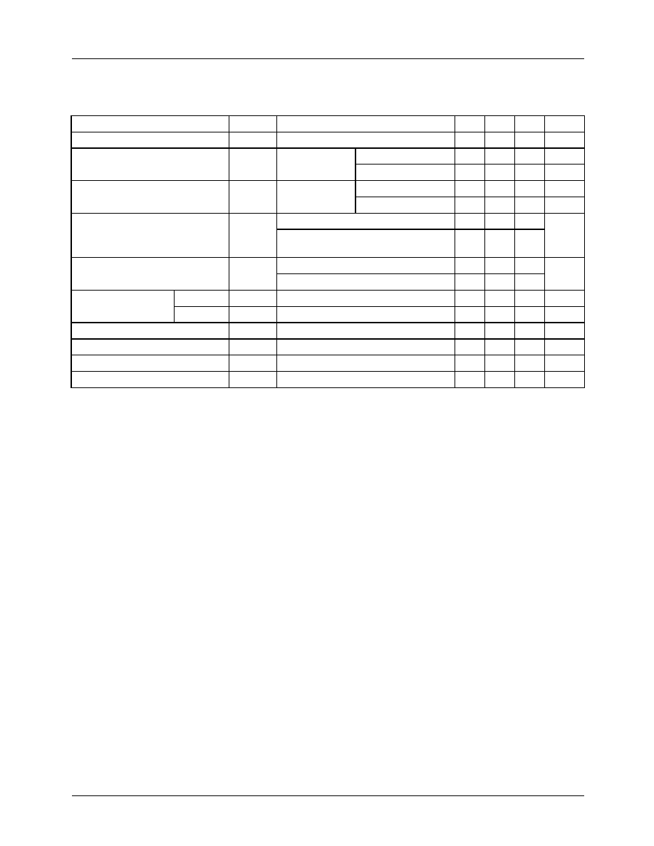
Absolute Maximum Ratings
Electrical Characteristics(KA78L05A)
(V
I
= 10V, I
O
= 40mA, 0
∞
C
T
J
125
∞
C, C
I
= 0.33
µ
F, C
O
= 0.1
µ
F, unless otherwise specified. (Note1)
Note:
1. The maximum steady state usable output current and input voltage are very dependent on the heat sinking and/or lead length
of the package. The data above represent pulse test conditions with junction temperature as indicated at the initiation of tests.
2. Power dissipation P
D
0.75W.
Parameter
Symbol
Value
Unit
Input Voltage (for V
O
= 5V, 8V)
(for V
O
= 12V to 18V)
(for V
O
=
24V
V
I
30
35
40
V
V
V
Operating Junction Temperature Range
T
J
0 ~ +150
∞
C
Storage Temperature Range
T
STG
-65 ~ +150
∞
C
Parameter
Symbol
Conditions
Min.
Typ. Max.
Unit
Output Voltage
V
O
T
J
= 25
∞
C
4.8
5.0
5.2
V
Line Regulation (Note1)
V
O
T
J
= 25
∞
C
7V
V
I
20V
-
8
150
mV
8V
V
I
20V
-
6
100
mV
Load Regulation (Note1)
V
O
T
J
= 25
∞
C
1mA
I
O
100mA
-
11
60
mV
1mA
I
O
40mA
-
5.0
30
mV
Output Voltage
V
O
7V
V
I
20V
1mA
I
O
40mA
-
-
5.25
V
7V
V
I
V
MAX
(Note2)
1mA
I
O
70mA
4.75
-
5.25
V
Quiescent Current
I
Q
T
J
= 25
∞
C
-
2.0
5.5
mA
Quiescent Current
Change
With Line
I
Q
8V
V
I
20V
-
-
1.5
mA
With Load
I
Q
1mA
I
O
40
mA
-
-
0.1
mA
Output Noise Voltage
V
N
T
A
= 25
∞
C, 10Hz
f
100kHz
-
40
-
µ
V/Vo
Temperature Coefficient of V
O
V
O
/
T
I
O
= 5mA
-
-0.65
-
mV/
∞
C
Ripple Rejection
RR
f = 120Hz, 8V
V
I
18V, T
J
= 25
∞
C
41
80
-
dB
Dropout Voltage
V
D
T
J
= 25
∞
C
-
1.7
-
V
KA78LXXA/KA78L05AA
3
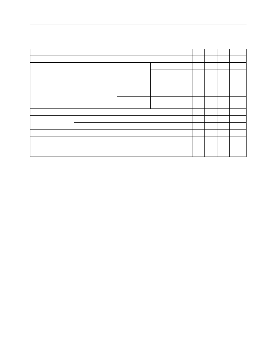
Electrical Characteristics(KA78L06A)
(Continued)
(V
I
= 12V, I
O
= 40mA, 0
∞
C
T
J
125
∞
C, C
I
= 0.3
3
µ
F, C
O
= 0.1
µ
F, unless otherwise specified. (Note 1)
Note:
1. The maximum steady state usable output current and input voltage are very dependent on the heat sinking and/or lead length
of the package. The data above represent pulse test conditions with junction temperature as indicated at the initiation of tests.
2. Power dissipation P
D
0.75W.
Parameter
Symbol
Conditions
Min. Typ. Max.
Unit
Output Voltage
V
O
T
J
= 25
∞
C
5.75
6.0
6.25
V
Line Regulation (Note1)
V
O
T
J
= 25
∞
C
8.5V
V
I
20V
-
64
175
mV
9V
V
I
20V
-
54
125
mV
Load Regulation (Note1)
V
O
T
J
= 25
∞
C
1mA
I
O
100mA
-
12.8
80
mV
1mA
I
O
70mA
-
5.8
40
mV
Output Voltage
V
O
8.5
V
I
20V, 1mA
I
O
40mA
5.7
-
6.3
V
8.5
V
I
V
MAX
(Note), 1mA
I
O
70mA 5.7
-
6.3
V
Quiescent Current
I
Q
T
J
= 25
∞
C
-
-
5.5
mA
T
J
= 125
∞
C
-
3.9
6.0
mA
Quiescent Current
Change
With Line
I
Q
9
V
I
20V
-
-
1.5
mA
With Load
I
Q
1mA
I
O
40mA
-
-
0.1
mA
Output Noise Voltage
V
N
T
A
= 25
∞
C, 10Hz
f
100kHz
-
40
-
µ
V/Vo
Temperature Coefficient of V
O
V
O
/
T
I
O
= 5mA
-
0.75
-
mV/
∞
C
Ripple Rejection
RR
f = 120Hz, 10V
V
I
20V, T
J
= 25
∞
C
40
46
-
dB
Dropout Voltage
V
D
T
J
= 25
∞
C
-
1.7
-
V
KA78LXXA/KA78L05AA
4
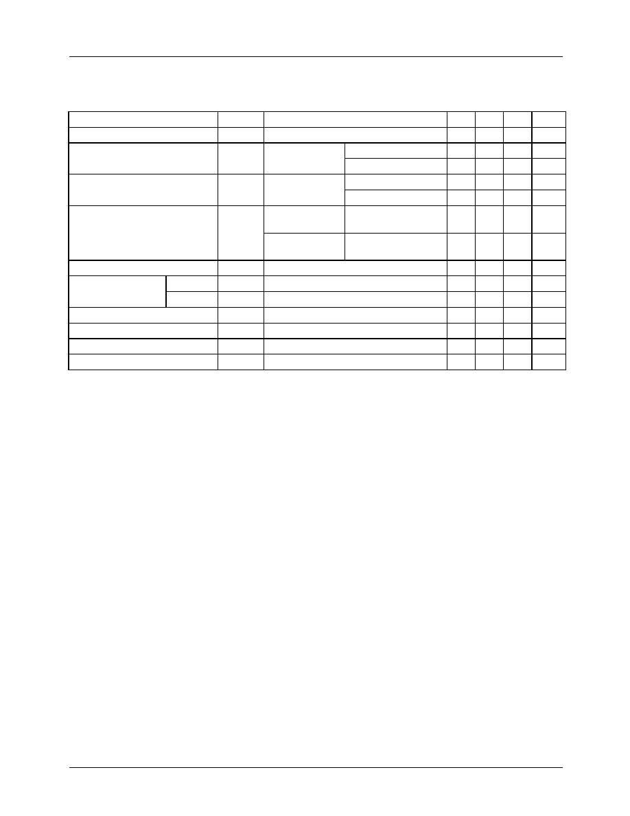
Electrical Characteristics(KA78L08A)
(Continued)
(V
I
= 14V, I
O
= 40mA, 0
∞
C
T
J
125
∞
C, C
I
= 0.33
µ
F, C
O
= 0.1
µ
F, unless otherwise specified. (Note1)
Note:
1. The maximum steady state usable output current and input voltage are very dependent on the heat sinking and/or lead length
of the package. The data above represent pulse test conditions with junction temperature as indicated at the initiation of tests.
2. Power dissipation P
D
0.75W.
Parameter
Symbol
Conditions
Min. Typ. Max.
Unit
Output Voltage
V
O
T
J
= 25
∞
C
7.7
8.0
8.3
V
Line Regulation (Note1)
V
O
T
J
= 25
∞
C
10.5V
V
I
23V
-
10
175
mV
11V
V
I
23V
-
8
125
mV
Load Regulation (Note1)
V
O
T
J
= 25
∞
C
1mA
I
O
100mA
-
15
80
mV
1mA
I
O
40mA
-
8.0
40
mV
Output Voltage
V
O
10.5V
V
I
23V 1mA
I
O
40mA
7.6
-
8.4
V
10.5V
V
I
V
MAX
(Note2)
1mA
I
O
70mA
7.6
-
8.4
V
Quiescent Current
I
Q
T
J
= 25
∞
C
-
2.0
5.5
mA
Quiescent Current
Change
With Line
I
Q
11V
V
I
23V
-
-
1.5
mA
With Load
I
Q
1mA
I
O
40mA
-
-
0.1
mA
Output Noise Voltage
V
N
T
A
= 25
∞
C, 10Hz
f
100kHz
-
60
-
µ
V/Vo
Temperature Coefficient of V
O
V
O
/
T
I
O
= 5mA
-
-0.8
-
mV/
∞
C
Ripple Rejection
RR
f = 120Hz, 11V
V
I
21V, T
J
= 25
∞
C
39
70
-
dB
Dropout Voltage
V
D
T
J
= 25
∞
C
-
1.7
-
V
KA78LXXA/KA78L05AA
5
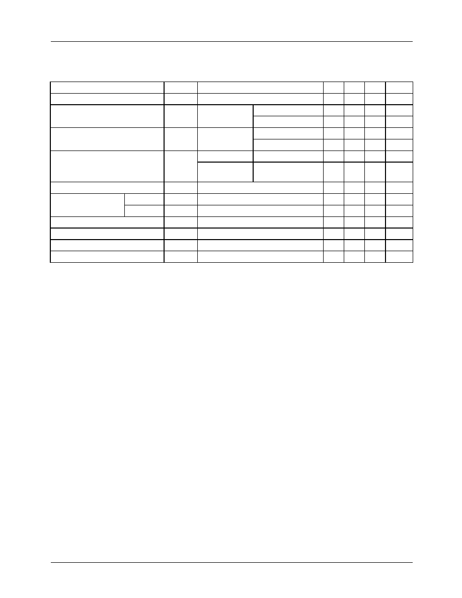
Electrical Characteristics(KA78L09A)
(Continued)
(V
I
= 15V, I
O
= 40mA, 0
∞
C
T
J
125
∞
C, C
I
= 0.33
µ
F, C
O
= 0.
1
µ
F, unless otherwise specified. (Note1)
Note:
1. The maximum steady state usable output current and input voltage are very dependent on the heat sinking and/or lead length
of the package. The data above represent pulse test conditions with junction temperature as indicated at the initiation of tests.
2. Power dissipation P
D
0.75W.
Parameter
Symbol
Conditions
Min. Typ. Max.
Unit
Output Voltage
V
O
T
J
= 25
∞
C
8.64
9.0
9.36
V
Line Regulation (Note1)
V
O
T
J
= 25
∞
C
11.5V
V
I
24V
-
90
200
mV
13V
V
I
24V
-
100
150
mV
Load Regulation (Note1)
V
O
T
J
= 25
∞
C
1mA
I
O
100mA
-
20
90
mV
1mA
I
O
40mA
-
10
45
mV
Output Voltage
V
O
11.5V
V
I
24V 1mA
I
O
40mA
8.55
-
9.45
V
11.5V
V
I
V
MAX
(Note 2)
1mA
I
O
70mA
8.55
-
9.45
V
Quiescent Current
I
Q
T
J
= 25
∞
C
-
2.1
6.0
mA
Quiescent Current
Change
With Line
I
Q
13V
V
I
24V
-
-
1.5
mA
With Load
I
Q
1mA
I
O
40mA
-
-
0.1
mA
Output Noise Voltage
V
N
T
A
= 25
∞
C, 10Hz
f
100kHz
-
70
-
µ
V/Vo
Temperature Coefficient of V
O
V
O
/
T
I
O
= 5mA
-
-0.9
-
mV/
∞
C
Ripple Rejection
RR
f = 120Hz, 12V
V
I
22V, T
J
= 25
∞
C
38
44
-
dB
Dropout Voltage
V
D
T
J
= 25
∞
C
-
1.7
-
V
KA78LXXA/KA78L05AA
6
Electrical Characteristics(KA78L10A)
(Continued)
(V
I
= 16V, I
O
= 40mA, 0
∞
C
T
J
125
∞
C, C
I
= 0.33
µ
F, C
O
= 0.
1
µ
F, unless otherwise specified. (Note1)
Notes:
1. The maximum steady state usable output current and input voltage are very dependent on the heat sinking and/or lead length
of the package. The data above represent pulse test conditions with junction temperature as indicated at the initiation of tests.
2. Power dissipation P
D
0.75W.
Parameter
Symbol
Conditions
Min. Typ. Max.
Unit
Output Voltage
V
O
T
J
= 25
∞
C
9.6
10.0 10.4
V
Line Regulation (Note1)
V
O
T
J
= 25
∞
C
12.5
V
I
25V
-
100
220
mV
14V
V
I
25V
-
100
170
mV
Load Regulation (Note1)
V
O
T
J
= 25
∞
C
1mA
I
O
100mA
-
20
94
mV
1mA
I
O
70mA
-
10
47
mV
Output Voltage
V
O
12.5V
V
I
25V, 1mA
I
O
40mA
9.5
-
10.5
V
12.5V
V
I
V
MAX
(Note2)
1mA
I
O
70mA
9.5
-
10.5
Quiescent Current
I
Q
T
J
= 25
∞
C -
-
6.0
mA
T
J
=125
∞
C
-
4.2
6.5
Quiescent Current
Change
With Line
I
Q
12.5
V
I
25V
-
-
1.5
mA
With Load
I
Q
1mA
I
O
40mA
-
-
0.1
mA
Output Noise Voltage
V
N
T
A
= 25
∞
C, 10Hz
f
100kHz
-
74
-
µ
V/Vo
Temperature Coefficient of V
O
V
O
/
T
I
O
= 5mA
-
0.95
-
mV/
∞
C
Ripple Rejection
RR
f = 120Hz, 15V
V
I
25V, T
J
= 25
∞
C
38
43
-
dB
Dropout Voltage
V
D
T
J
= 25
∞
C
-
1.7
-
V
KA78LXXA/KA78L05AA
7
Electrical Characteristics(KA78L12A)
(Continued)
(V
I
= 19V, I
O
= 40mA, 0
∞
C
T
J
125
∞
C, C
I
= 0.33
µ
F, C
O
= 0.
1
µ
F, unless otherwise specified. (Note 1)
Note:
1. The maximum steady state usable output current and input voltage are very dependent on the heat sinking and/or lead length
of the package. The data above represent pulse test conditions with junction temperature as indicated at the initiation of tests.
2. Power dissipation P
D
0.75W.
Parameter
Symbol
Conditions
Min. Typ. Max.
Unit
Output Voltage
V
O
T
J
= 25
∞
C
11.5
12
12.5
V
Line Regulation (Note1)
V
O
T
J
= 25
∞
C
14.5V
V
I
27V
-
20
250
mV
16V
V
I
27V
-
15
200
mV
Load Regulation (Note1)
V
O
T
J
= 25
∞
C
1mA
I
O
100mA
-
20
100
mV
1mA
I
O
40mA
-
10
50
mV
Output Voltage
V
O
14.5V
V
I
27V 1mA
I
O
40mA
11.4
-
12.6
V
14.5V
V
I
V
MAX
(Note 2)
1mA
I
O
70mA
11.4
-
12.6
V
Quiescent Current
I
Q
T
J
= 25
∞
C
-
2.1
6.0
mA
Quiescent Current
Change
With Line
I
Q
16V
V
I
27V
-
-
1.5
mA
With Load
I
Q
1mA
I
O
40mA
-
-
0.1
mA
Output Noise Voltage
V
N
T
A
= 25
∞
C, 10Hz
f
100kHz
-
80
-
µ
V/Vo
Temperature Coefficient of V
O
V
O
/
T
I
O
= 5mA
-
-1.0
-
mV/
∞
C
Ripple Rejection
RR
f = 120Hz, 15V
V
I
25V, T
J
= 25
∞
C
37
65
-
dB
Dropout Voltage
V
D
T
J
= 25
∞
C
-
1.7
-
V
KA78LXXA/KA78L05AA
8
Electrical Characteristics(KA78L15A)
(Continued)
(V
I
= 23V, I
O
= 40mA, 0
∞
C
T
J
125
∞
C, C
I
= 0.33
µ
F, C
O
= 0.
1
µ
F, unless otherwise specified. (Note1)
Note:
1. The maximum steady state usable output current and input voltage are very dependent on the heat sinking and/or lead length
of the package. The data above represent pulse test conditions with junction temperature as indicated at the initiation of tests.
2. Power dissipation P
D
0.75W.
Parameter
Symbol
Conditions
Min. Typ. Max. Unit
Output Voltage
V
O
T
J
= 25
∞
C
14.4
15
15.6
V
Line Regulation (Note1)
V
O
T
J
= 25
∞
C
17.5V
V
I
30V
-
25
300
mV
20V
V
I
30V
-
20
250
mV
Load Regulation (Note1)
V
O
T
J
= 25
∞
C
1mA
I
O
100mA
-
25
150
mV
1mA
I
O
40mA
-
12
75
mV
Output Voltage
V
O
17.5V
V
I
30V
1mA
I
O
40mA
14.2
5
-
15.7
5
V
17.5V
V
I
V
MAX
(Note 2)
1mA
I
O
70mA
14.2
5
-
15.7
5
V
Quiescent Current
I
Q
T
J
= 25
∞
C
-
2.1
6.0
mA
Quiescent Current
Change
With Line
I
Q
20V
V
I
30V
-
-
1.5
mA
With Load
I
Q
1mA
I
O
40mA
-
-
0.1
mA
Output Noise Voltage
V
N
T
A
= 25
∞
C, 10Hz
f
100kHz
-
90
-
µ
V/Vo
Temperature Coefficient of V
O
V
O
/
T
I
O
= 5mA
-
-1.3
-
mV/
∞
C
Ripple Rejection
RR
f = 120Hz, 18.5V
V
I
28.5V, T
J
= 25
∞
C 34
60
-
dB
Dropout Voltage
V
D
T
J
= 25
∞
C
-
1.7
-
V
KA78LXXA/KA78L05AA
9
Electrical Characteristics(KA78L18A)
(Continued)
(V
I
= 27V, I
O
= 40mA, 0
∞
C
T
J
125
∞
C, C
I
= 0.33
µ
F, C
O
= 0.
1
µ
F, unless otherwise specified. (Note1)
Note:
1. The maximum steady state usable output current and input voltage are very dependent on the heat sinking and/or lead length
of the package. The data above represent pulse test conditions with junction temperature as indicated at the initiation of tests.
2. Power dissipation P
D
0.75W.
Parameter
Symbol
Conditions
Min. Typ. Max.
Unit
Output Voltage
V
O
T
J
= 25
∞
C
17.3
18
18.7
V
Line Regulation (Note1)
V
O
T
J
= 25
∞
C
21V
V
I
33V
-
145
300
mV
22V
V
I
33V
-
135
250
mV
Load Regulation (Note1)
V
O
T
J
= 25
∞
C
1mA
I
O
100mA
-
30
170
mV
1mA
I
O
40mA
-
15
85
mV
Output Voltage
V
O
21V
V
I
33V
1mA
I
O
40mA
17.1
-
18.9
V
21V
V
I
V
MAX
(Note 2)
1mA
I
O
70mA
17.1
-
18.9
V
Quiescent Current
I
Q
T
J
= 25
∞
C
-
2.2
6.0
mA
Quiescent Current
Change
With Line
I
Q
21V
V
I
33V
-
-
1.5
mA
With Load
I
Q
1mA
I
O
40mA
-
-
0.1
mA
Output Noise Voltage
V
N
T
A
= 25
∞
C, 10Hz
f
100kHz
-
150
-
µ
V/Vo
Temperature Coefficient of V
O
V
O
/
T
I
O
= 5mA
-
-1.8
-
mV/
∞
C
Ripple Rejection
RR
f = 120Hz, 23V
V
I
33V, T
J
= 25
∞
C
34
48
-
dB
Dropout Voltage
V
D
T
J
= 25
∞
C
-
1.7
-
V

KA78LXXA/KA78L05AA
10
Electrical Characteristics(KA78L24A)
(Continued)
(V
I
= 33V, I
O
= 40mA, 0
∞
C
T
J
125
∞
C, C
I
= 0.33
µ
F, C
O
= 0.
1
µ
F, unless otherwise specified. (Note1)
Note:
1. The maximum steady state usable output current and input voltage are very dependent on the heat sinking and/or lead length
of the package. The data above represent pulse test conditions with junction temperature as indicated at the initiation of tests.
2. Power dissipation P
D
0.75W.
Parameter
Symbol
Conditions
Min. Typ. Max.
Unit
Output Voltage
V
O
T
J
= 25
∞
C
23
24
25
V
Line Regulation (Note1)
V
O
T
J
= 25
∞
C
27V
V
I
38V
-
160
300
mV
28V
V
I
38V
-
150
250
mV
Load Regulation (Note1)
V
O
T
J
= 25
∞
C
1mA
I
O
100mA
-
40
200
mV
1mA
I
O
40mA
-
20
100
mV
Output Voltage
V
O
27V
V
I
38V
1mA
I
O
40mA
22.8
-
25.2
V
27V
V
I
V
MAX
(Note2)
1mA
I
O
70mA
22.8
-
25.2
V
Quiescent Current
I
Q
T
J
= 25
∞
C
-
2.2
6.0
mA
Quiescent Current
Change
With Line
I
Q
28V
V
I
38V
-
-
1.5
mA
With Load
I
Q
1mA
I
O
40mA
-
-
0.1
mA
Output Noise Voltage
V
N
T
A
= 25
∞
C, 10Hz
f
100kHz
-
200
-
µ
V/Vo
Temperature Coefficient of V
O
V
O
/
T
I
O
= 5mA
-
-2.0
-
mV/
∞
C
Ripple Rejection
RR
f = 120Hz, 28V
V
I
38V, T
J
= 25
∞
C
34
45
-
dB
Dropout Voltage
V
D
T
J
= 25
∞
C
-
1.7
-
V

KA78LXXA/KA78L05AA
11
Absolute Maximum Ratings
Electrical Characteristics(KA78L05AA)
(Continued)
(V
I
= 10V, I
O
= 40mA, 0
∞
C
T
J
125
∞
C, C
I
= 0.33
µ
F, C
O
= 0.
1
µ
F, unless otherwise specified. (Note1)
Note:
1. The maximum steady state usable output current and input voltage are very dependent on the heat sinking and/or lead length
of the package. The data above represent pulse test conditions with junction temperature as indicated at the initiation of tests.
2. Power dissipation P
D
0.75W.
Parameter
Symbol
Value
Unit
Input Voltage (for V
O
= 5V, 8V)
(for V
O
= 12V to 18V)
(for V
O
=
24V
V
I
30
35
40
V
V
V
Operating Junction Temperature Range
T
J
0 ~ +150
∞
C
Storage Temperature Range
T
STG
-65 ~ +150
∞
C
Parameter
Symbol
Conditions
Min.
Typ. Max.
Unit
Output Voltage
V
O
T
J
= 25
∞
C
4.9
5.0
5.1
V
Line Regulation (Note1)
V
O
T
J
= 25
∞
C
7V
V
I
20V
-
8
150
mV
8V
V
I
20V
-
6
100
mV
Load Regulation (Note1)
V
O
T
J
= 25
∞
C
1mA
I
O
100mA
-
11
50
mV
1mA
I
O
40mA
-
5.0
25
mV
Output Voltage
V
O
7V
V
I
20V
1mA
I
O
40mA
-
-
5.15
V
7V
V
I
V
MAX
(Note2)
1mA
I
O
70mA
4.85
-
5.15
V
Quiescent Current
I
Q
T
J
= 25
∞
C
-
2.0
5.5
mA
Quiescent Current
Change
With Line
I
Q
8V
V
I
20V
-
-
1.5
mA
With Load
I
Q
1mA
I
O
40
mA
-
-
0.1
mA
Output Noise Voltage
V
N
T
A
= 25
∞
C, 10Hz
f
100kHz
-
40
-
µ
V/Vo
Temperature Coefficient of V
O
V
O
/
T
I
O
= 5mA
-
-0.65
-
mV/
∞
C
Ripple Rejection
RR
f = 120Hz, 8V
V
I
18V, T
J
= 25
∞
C
41
80
-
dB
Dropout Voltage
V
D
T
J
= 25
∞
C
-
1.7
-
V
KA78LXXA/KA78L05AA
12
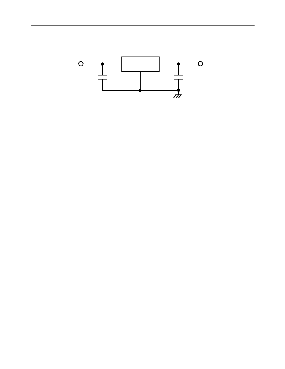
Typical Application
'( )' : 8SOP Type
Note:
1. To specify an output voltage, substitute voltage value for "XX".
2. Bypass Capacitors are recommend for optimum stability and transient response and should be located as close as possible
to the regulator
KA78LXXA
NOTE 1
INPUT
OUTPUT
1(1)
2(2,3,6,7)
3(8)
C1
0.33
µ
F
NOTE 2
0. 1
NOTE 2
µ
F
KA78LXXA/KA78L05AA
13
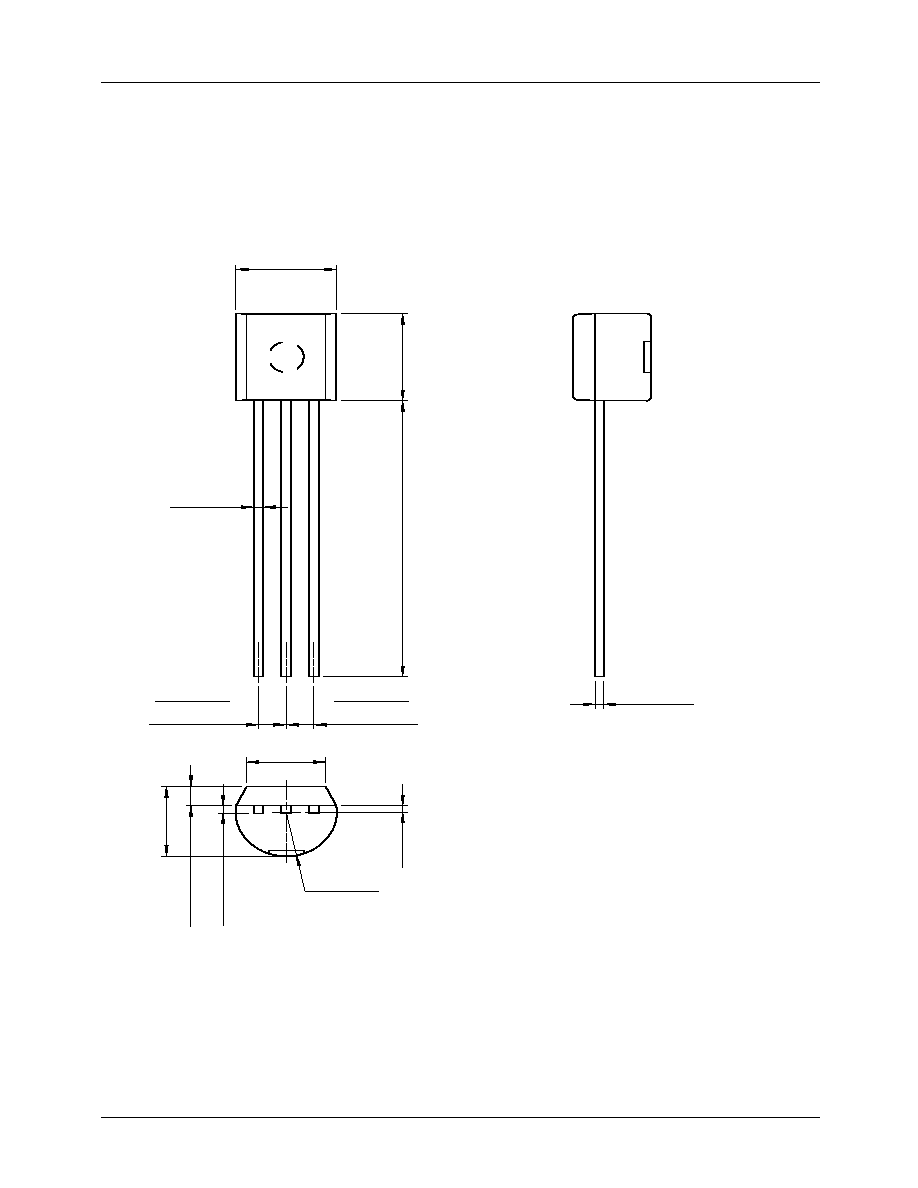
Mechanical Dimensions
Package
Dimensions in millimeters
0.46
±
0.10
1.27TYP
(R2.29)
3.86MAX
[1.27
±
0.20
]
1.27TYP
[1.27
±
0.20
]
3.60
±
0.20
14.47
±
0.40
1.02
±
0.10
(0.25)
4.58
±
0.20
4.58
+0.25
≠0.15
0.38
+0.10
≠0.05
0.38
+0.10
≠0.05
TO-92
KA78LXXA/KA78L05AA
14
Mechanical Dimensions
(Continued)
Package
Dimensions in millimeters
Symbol
Min
Nom
Max
A
-
-
1.75
A1
0.10
0.15
0.25
A2
1.25
1.45
1.50
B
0.35
0.37
0.51
C
0.19
0.20
0.25
D
4.80
4.90
5.00
E
3.80
3.90
4.00
e
1.27BSC
H
5.79
5.99
6.20
h
0.25
-
0.50
L
0.50
0.70
0.90
GP
0.36 BSC
q
0
-
8
aaa
-
-
0.25
bbb
-
-
0.10
8-SOP
KA78LXXA/KA78L05AA
15
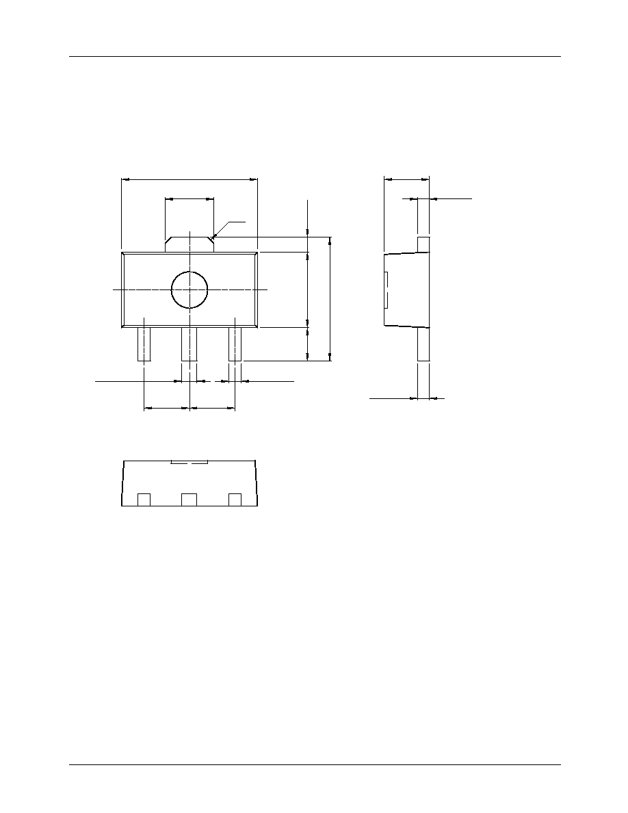
Mechanical Dimensions
(Continued)
Package
Dimensions in millimeters
SOT-89
0.40
±
0.10
2.50
±
0.20
(0.50)
(0.40)
4.10
±
0.20
0.40
+0.10
≠0.05
0.50
±
0.10
1.65
±
0.10
4.50
±
0.20
1.50
±
0.20
C0.2
1.50 TYP 1.50 TYP
(1.10)

KA78LXXA/KA78L05AA
16
Ordering Information
Note:
1. For information on tape & reel and ammo pack specifications, including part orientation and tape sizes, please refer to our tape
and reel data, www.fairchildsemi.com/products/analog/pdf/to92r_tr.pdf.
Product Number
Package
Packing
Output Voltage Tolerance Operating Temperature
KA78L05AZTA
TO-92
Ammo
5%
0 ~ +125
∞
C
KA78L05AZTF
Tape & Reel
KA78L05AZBU
Bulk
KA78L06AZTA
Ammo
KA78L06AZBU
Tape & Reel
KA78L08AZTA
Ammo
KA78L08AZTF
Tape & Reel
KA78L08AZBU
Bulk
KA78L09AZTA
Ammo
KA78L09AZBU
Tape & Reel
KA78L10AZTA
Ammo
KA78L10AZBU
Tape & Reel
KA78L12AZTA
Ammo
KA78L12AZTF
Tape & Reel
KA78L12AZBU
Bulk
KA78L15AZTA
Ammo
KA78L15AZBU
Tape & Reel
KA78L18AZTA
Ammo
KA78L18AZBU
Tape & Reel
KA78L24AZTA
Ammo
KA78L05AMTF
SOT-89
Tape & Reel
KA78L05AMTM
Tape & Reel
KA78L08AMTF
Tape & Reel
KA78L09AMTF
Tape & Reel
KA78L12AMTF
Tape & Reel
KA78L05AD
8-SOP
Tube
KA78L05ADTF
Tape & Reel
KA78L08AD
Tube
KA78L08ADTF
Tape & Reel
KA78L12AD
Tube
KA78L12ADTF
Tape & Reel
KA78L05AAZTA
TO-92
Ammo
2%
KA78L05AAZBU
Bulk

KA78LXXA/KA78L05AA
17

KA78LXXA/KA78L05AA
5/17/05 0.0m 001
Stock#DSxxxxxxxx
2005 Fairchild Semiconductor Corporation
LIFE SUPPORT POLICY
FAIRCHILD'S PRODUCTS ARE NOT AUTHORIZED FOR USE AS CRITICAL COMPONENTS IN LIFE SUPPORT DEVICES
OR SYSTEMS WITHOUT THE EXPRESS WRITTEN APPROVAL OF THE PRESIDENT OF FAIRCHILD SEMICONDUCTOR
CORPORATION. As used herein:
1. Life support devices or systems are devices or systems
which, (a) are intended for surgical implant into the body,
or (b) support or sustain life, and (c) whose failure to
perform when properly used in accordance with
instructions for use provided in the labeling, can be
reasonably expected to result in a significant injury of the
user.
2. A critical component in any component of a life support
device or system whose failure to perform can be
reasonably expected to cause the failure of the life support
device or system, or to affect its safety or effectiveness.
www.fairchildsemi.com
DISCLAIMER
FAIRCHILD SEMICONDUCTOR RESERVES THE RIGHT TO MAKE CHANGES WITHOUT FURTHER NOTICE TO ANY
PRODUCTS HEREIN TO IMPROVE RELIABILITY, FUNCTION OR DESIGN. FAIRCHILD DOES NOT ASSUME ANY
LIABILITY ARISING OUT OF THE APPLICATION OR USE OF ANY PRODUCT OR CIRCUIT DESCRIBED HEREIN; NEITHER
DOES IT CONVEY ANY LICENSE UNDER ITS PATENT RIGHTS, NOR THE RIGHTS OF OTHERS.