©2003 Fairchild Semiconductor Corporation
www.fairchildsemi.com
Rev. 1.0.0
Features
∑ 1A/3.3V, 5V, 8V, 9V, 12V, 15V output low dropout
voltage regulator
∑ TO-220 full-mold package (4pin)
∑ Overcurrent protection, thermal shutdown
∑ Overvoltage protection, short circuit protection
∑ With output disable function
Description
The KA78RXXC is a low-dropout voltage regulator suitable
for various electronic equipments.
It provides constant voltage power source with TO-220-4
lead full mold package. Dropout voltage of KA78RXXC is
below 0.5V in full rated current(1A).
This regulator has various functions such as peak current
protection, thermal shut down, overvoltage protection and
output disable function.
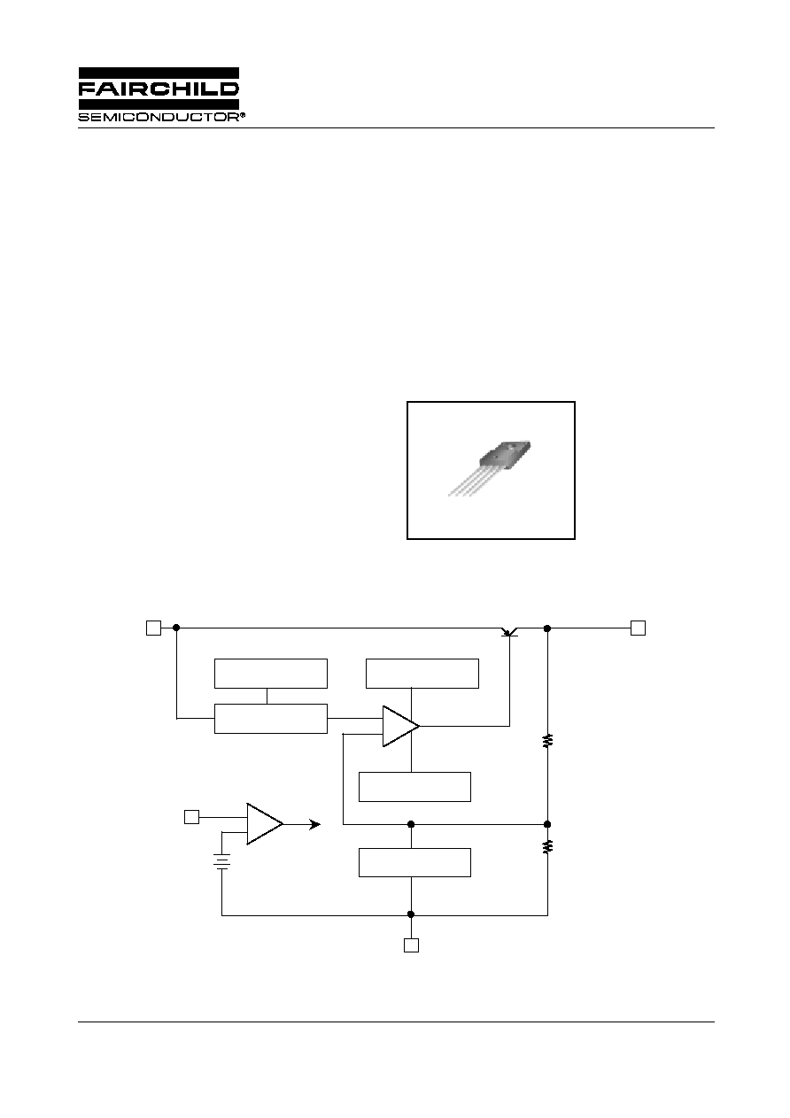
TO-220F-4L
1. Vin 2. V
O
3. GND 4. Vdis
1
Internal Block Diagram
THERMAL SHUTDOWN
BANDGAP REFERENCE
OVERVOLTAGE
PROTECTION
SOA PROTECTION
SHORTCIRCUIT
PROTECTION
1
4
3
2
Vin
Vdis
Vo
GND
HIGH / LOW
OUTPUT
ON / OFF
Q1
R1
R2
-
+
-
+
1.4V
SHORT-CIRCUIT
KA78RXXC-Series
1A Output Low Dropout Voltage Regulators
KA78RXXC-SERIES
2
Absolute Maximum Ratings
KA78RXXC
Parameter
Symbol
Value
Unit
Remark
Input voltage
Vin
35
V
-
Disable voltage
Vdis
35
V
-
Output current
Io
1.0
A
-
Power dissipation 1
Pd1
1.5
W
No heatsink
Power dissipation 2
Pd2
15
W
With heatsink
Junction temperature
Tj
+150
∞
C
-
Operating temperature
Topr
-20 ~ +80
∞
C
-
Thermal resistance, junction-to case (Note2)
R
jc
4.31
∞
C/W
-
Thermal resistance, junction-to-air (Note2)
R
ja
48.83
∞
C/W
-
KA78RXXC-SERIES
3
Electrical Characteristics
(Vin = Note3, Io = 0.5A, Ta = 25
∞
C, unless otherwise specified)
Note:
1.These parameters, although guaranteed, are not 100% tested in production.
2. Junction -to -case thermal resistance test environments.
-. Pneumatic heat sink fixture.
-. Clamping pressure 60psi through 12mm diameter cylinder.
-. Thermal grease applied between PKG and heat sink fixture.
3. KA78R33C :Vin = 5V
KA78R05C : Vin = 7V
KA78R08C : Vin = 10V
KA78R09C : Vin = 11V
KA78R12C : Vin = 15V
KA78R15C : Vin = 20V
4. KA78R33C :Vin = 4V to 10V
KA78R05C : Vin = 6V to 12V
KA78R08C : Vin = 9V to 25V
KA78R09C : Vin = 10V to 25V
KA78R12C : Vin = 13V to 29V
KA78R15C : Vin = 16V to 30V
Parameter
Symbol
Conditions
Min.
Typ.
Max.
Unit
Output voltage
KA78R33C
Vo
-
3.22
3.3
3.38
V
KA78R05C
-
4.88
5
5.12
KA78R08C
-
7.8
8
8.2
KA78R09C
-
8.78
9
9.22
KA78R12C
-
11.7
12
12.3
KA78R15C
-
14.6
15
15.4
Load regulation
Rload
5mA < Io < 1A
-
0.1
2.0
%
Line regulation
Rline
Note4
-
0.5
2.5
%
Ripple rejection ratio
RR
Note1
45
55
-
dB
Dropout voltage
Vdrop
Io = 1A
-
-
0.5
V
Disable voltage high
VdisH
Output active
2.0
-
-
V
Disable voltage low
VdisL
Output disabled
-
-
0.8
V
Disable bias current high
IdisH
Vdis = 2.7V
-
-
20
µ
A
Disable bias current low
IdisL
Vdis = 0.4V
-
-
-0.4
mA
Quiescent current
Iq
Io = 0A
-
-
10
mA
KA78RXXC-SERIES
4
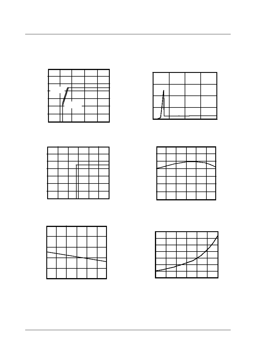
Typical Performance Characteristics
KA78R33
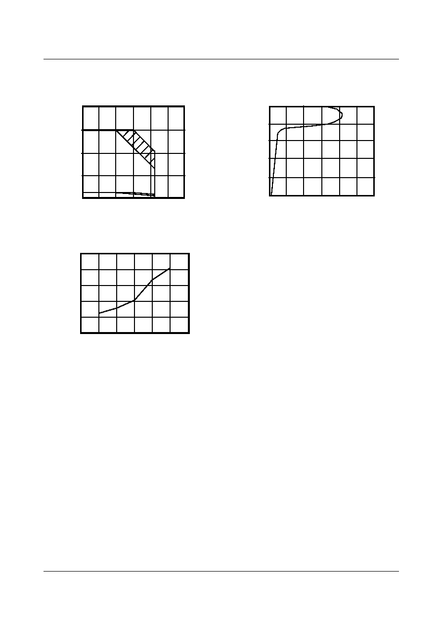
Figure 1. Output Voltage vs. Input Voltage
Figure 2. Quiescent Current vs. Input Voltage
Figure 3. Output Voltage vs. Disable Voltage
Figure 4. Output Voltage vs. Temperature(Tj)
Figure 5. Quiescent Current vs. Temperature(Tj)
Figure 6. Dropout Voltage vs.Junction Temperature
Input voltage Vin (V)
4.50
3.75
3.00
2.25
1.50
0.75
5.25
0
0 2 4 6 8 10
O
u
t
put voltage V
o
(V
)
RL=
RL=3.3
8
0
5
10
15
20
0
20
40
60
80
RL=
Q
u
i
e
scent cur
r
ent
I
q
(
m
A)
Input voltage Vin(V)
0
O
u
t
put
vo
l
t
a
ge
V
o
(
V
)
3
Disable voltage Vdis (V)
0.5
1.5
1
2
2.5
4.50
3.75
3.00
2.25
1.50
0.75
5.25
0
3.34
3.32
3.30
3.36
-25
O
u
tput
volta
ge
V
o
(V
)
TEMPERATURE Tj(
o
C)
75
125
0
25
50
100
3.26
3.24
3.22
3.28
10
8
6
4
2
0
Q
uescent current I
q
(
m
A
)
Junction temperature Tj(
o
C)
75
125
0
25
50
100
-25
-25
0
25
50
75
100
125
0.20
0.25
0.30
0.35
0.40
0.45
0.50
0.55
1.0A
D
r
op
ou
t
v
o
l
t
ag
e V
d
r
op
[
V
]
Junction Temp Tj [
]
KA78RXXC-SERIES
5
Typical Performance Characteristics
(Continued)
Figure 8. Overcurrent Protection Characteristics
(Typical Value)
Figure 7. Power Dissipation vs. Temperature(Tj)
-25
P
o
w
e
r dissipat
i
on P
D
(W)
TEMPERATURE T
J
(
o
C)
75
125
0
25
50
100
15
10
5
20
0
Output Current(A)
Rel
a
t
i
v
e
out
put
v
o
l
t
age(%
)
1.5
2.5
0
0.5
1.0
2.0
80
60
20
100
0
40
3.0
Output Current(A)
Rel
a
t
i
v
e
out
put
v
o
l
t
age(%
)
1.5
2.5
0
0.5
1.0
2.0
80
60
20
100
0
40
3.0
Rel
a
t
i
v
e
out
put
v
o
l
t
age(%
)
1.5
2.5
0
0.5
1.0
2.0
80
60
20
100
0
40
3.0
0
1
2
3
4
5
6
1.50
1.75
2.00
2.25
2.50
2.75
O
u
t
p
u
t
pea
k cu
r
r
ent
I
o
p (
A
)
Input-output differential voltage Vin-Vo (V)
Figure 9. Output Peak Currenrt vs.
Input-Output Differential Voltage