 | ÐлекÑÑоннÑй компоненÑ: KA8301-L | СкаÑаÑÑ:  PDF PDF  ZIP ZIP |
Äîêóìåíòàöèÿ è îïèñàíèÿ www.docs.chipfind.ru
©2000 Fairchild Semiconductor International
www.fairchildsemi.com
Rev. 1.0.1
February. 2000.
1
Features
· Built-in brake function.
· Built-in element to absorb a surge current derived from
changing motor direction and braking motor drive.
· External motor speed control pin
· Motor direction change circuit.
· Interfaces with CMOS devices.
Description
The KA8301 is a monolithic integrated circuit designed for
driving bi-directional DC motor with braking and speed con-
trol, and it is suitable for the loading motor driver of VCR
systems. The speed control can be achieved by adjusting the
external voltage of the speed control pin.
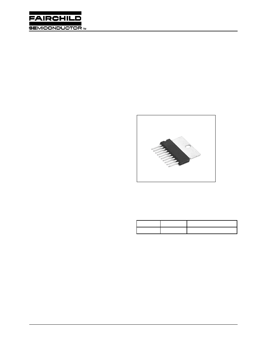
10-SIPH-B
Typical Application
· Video cassette recorder (VCR) loading motor
· Low current DC motor such audio or video equipment
· General DC motor
Ordering Information
Device
Package
Operating Temp.
KA8301-L
10-SIPH-B
-
25
°
C ~ +75
°
C
KA8301
Bi-Directional DC Motor Driver
KA8301
2
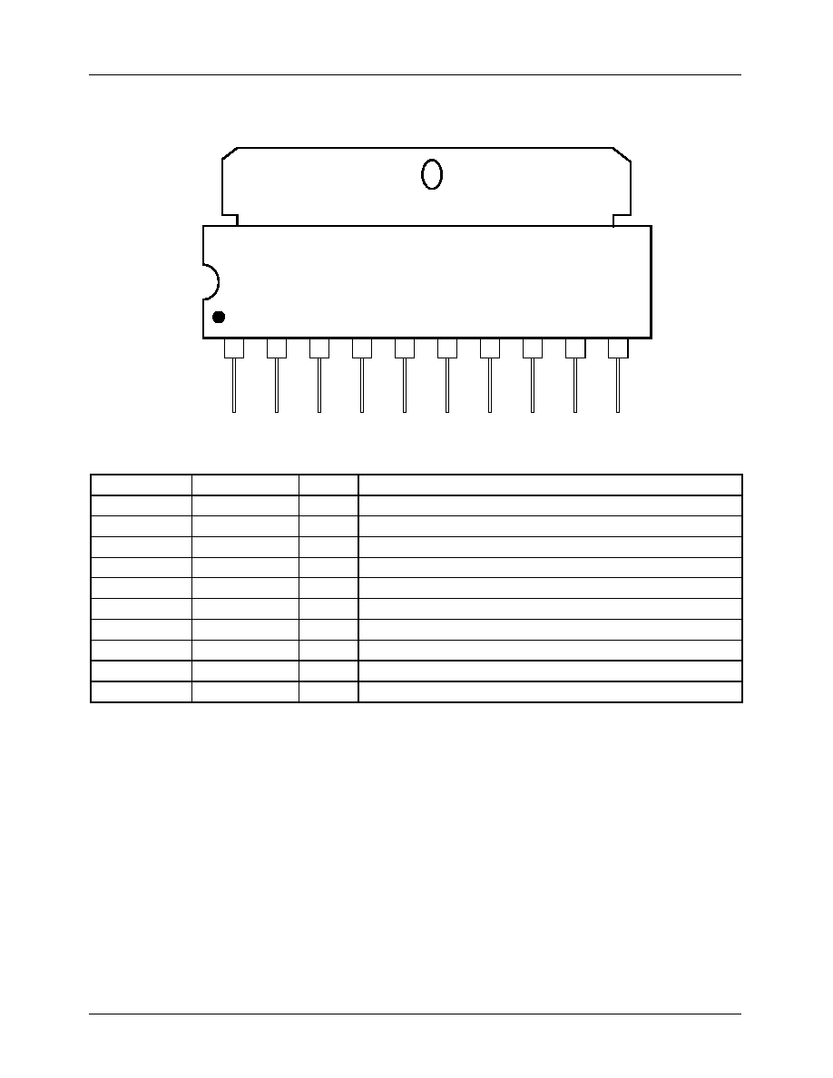
Pin Assignments
Pin Definitions
Pin Number
Pin Name
I/O
Pin Function Description
1
GND
-
Ground
2
V
OUT1
O
Output 1
3
V
Z1
-
Phase compensation
4
V
R
I
Motor speed control
5
F
IN
I
Input 1
6
R
IN
I
Input 2
7
V
CC1
-
Supply voltage (Signal)
8
V
CC2
I
Supply voltage (Power)
9
V
Z2
I
Phase compensation
10
V
OUT2
O
Output 2
1
2
3
4
5
6
7
8
9
10
GND
V
OUT1
V
Z1
V
R
F
IN
R
IN
V
CC1
V
OUT2
V
CC2
V
Z2
KA8301
KA8301
3
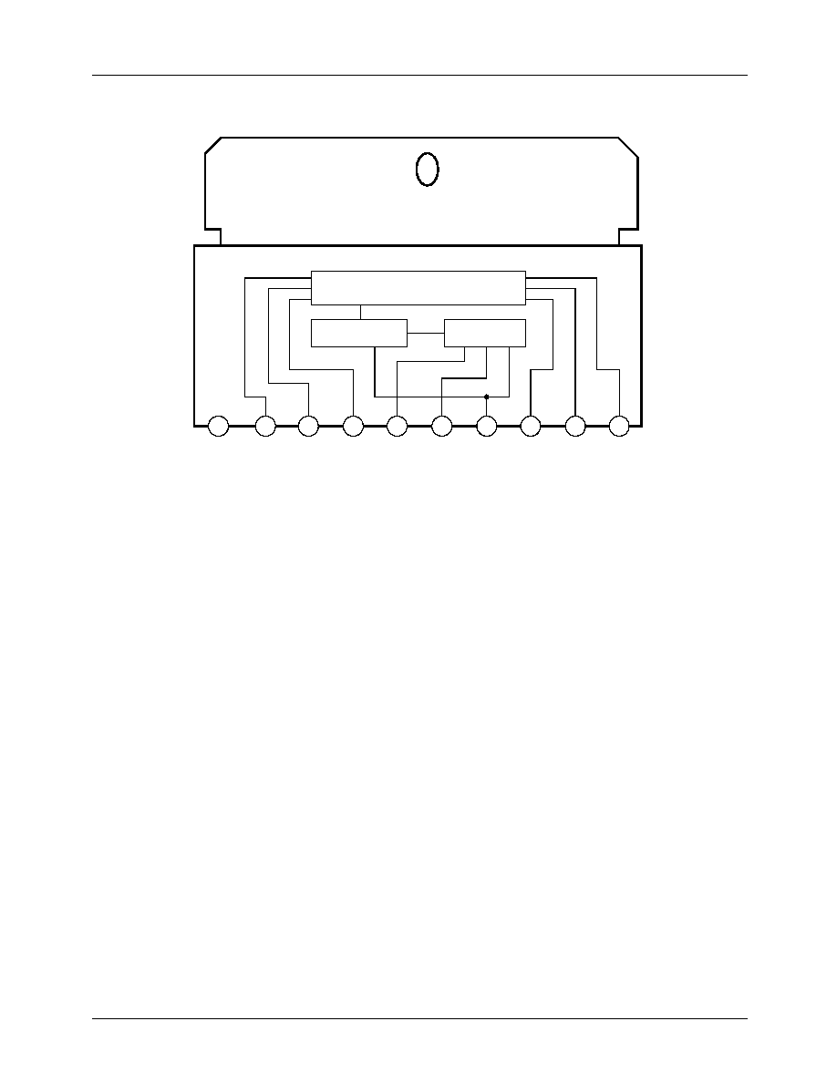
Internal Block Diagram
1
2
3
4
5
6
7
8
9
10
GND
V
OUT1
V
Z1
V
R
F
IN
R
IN
V
CC1
V
CC2
V
Z2
V
OUT2
LOGIC
PRE-DRIVER
DRIVER
KA8301
4
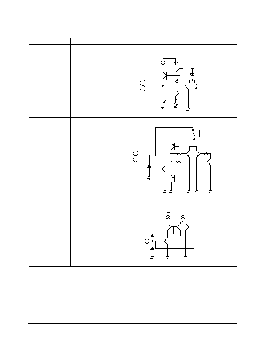
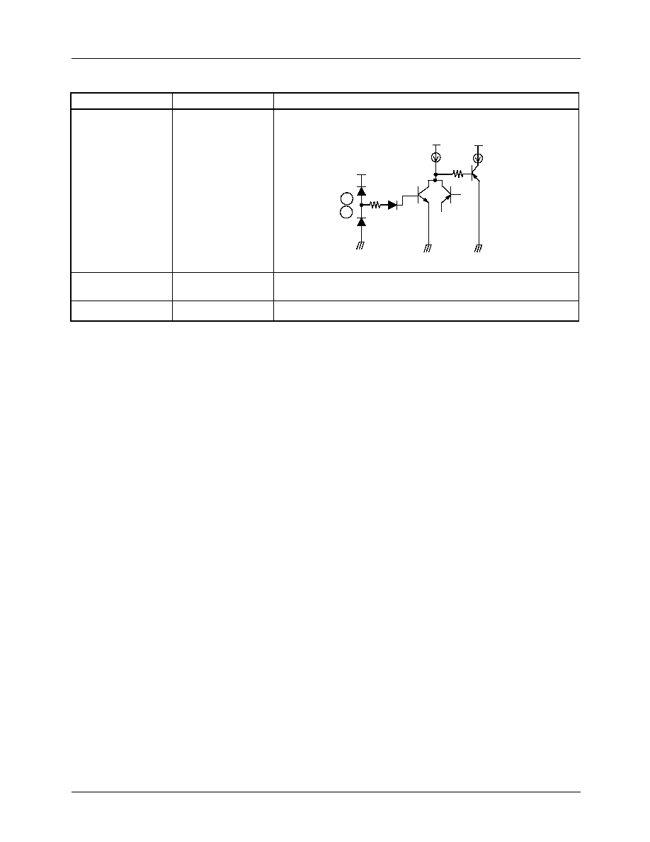
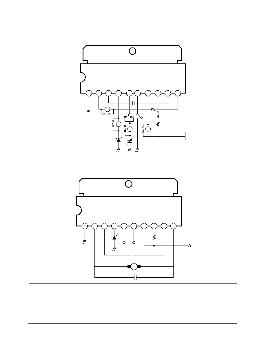
Equivalent Circuits
Description
Pin No.
Internal circuit
Output
2, 10
Phase
compensation
3, 9
Speed control
4
2
Vcc
Vcc
10
9
3
VCC
4
Vcc
Vcc
KA8301
5
Equivalent Circuit (Continued)
Description
Pin No.
Internal circuit
Input
5, 6
VCC1
VCC2
7
8
GND
1
5
6
VCC
Vcc
Vcc
KA8301
6
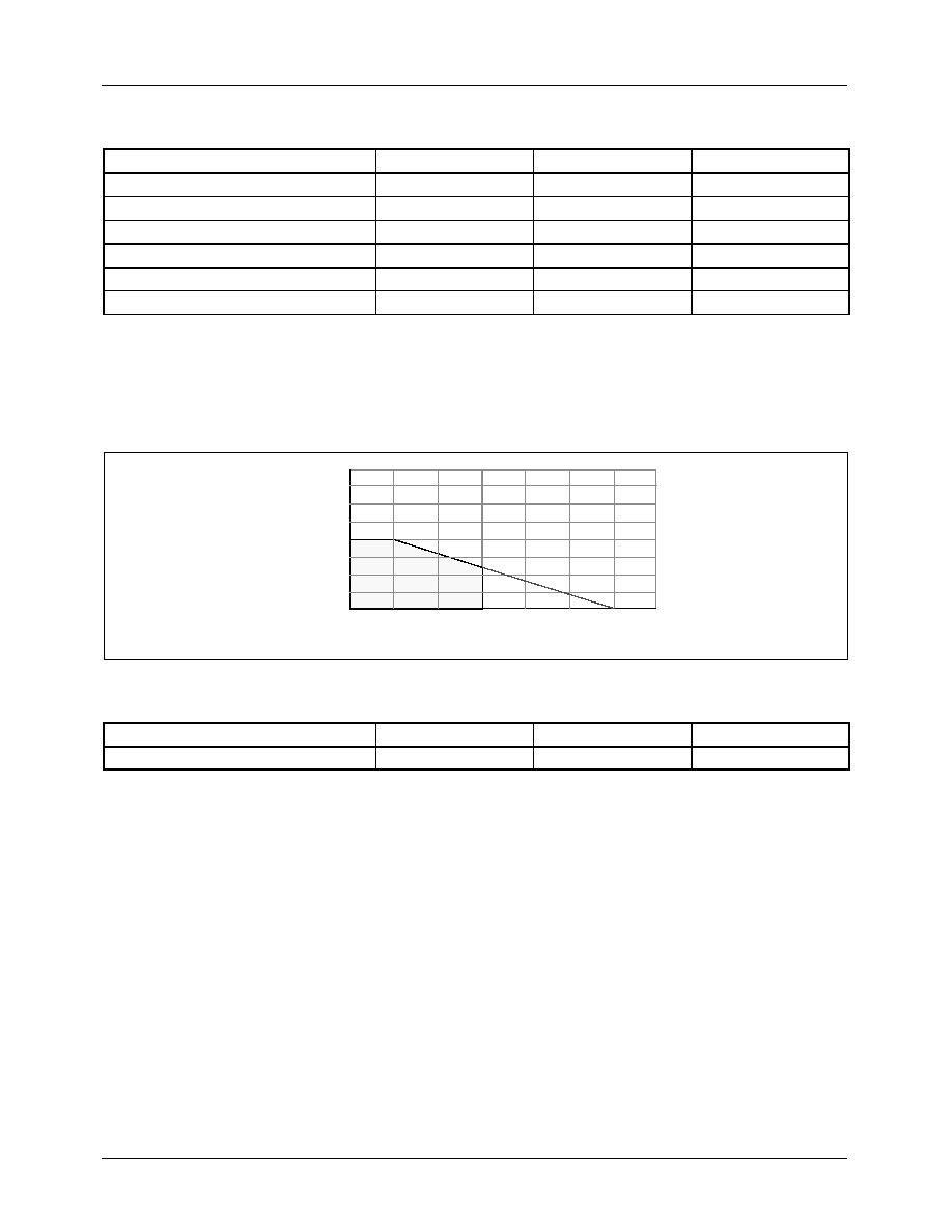
Absolute Maximum Ratings
(Ta=25
°
°
°
°
C)
Notes:
1. Duty 1/100, pulse width 500
µ
s
2. 1) When mounted on glass epoxy PCB (76.2
×
114
×
1.57mm)
2) Power dissipation reduces 120mW /
°
C for using above Ta=25
°
C
3) Do not exceed Pd and SOA(Safe Operating Area).
Power Dissipation Curve
Recommened Operating Conditions (Ta=25
°
°
°
°
C)
Parameter
Symbol
Value
Unit
Supply voltage
V
CCmax
18
V
Maximum output current
I
Omax
1.6
note1
A
Power dissipation
P
d
15
note2
W
Input voltage
V
IN
-
0.3 ~ V
CC
V
Operating temperature
T
OPR
-
25 ~ +75
°
C
Storage temperature
T
STG
-
55 ~ +150
°
C
Parameter
Symbol
Value
Unit
Operating supply voltage
V
CC
8 ~ 18
V
20
15
0
0
25
50
75
100
125
150
175
Pd (W)
Ambient temperature, Ta [
°
C]
SOA
KA8301
7
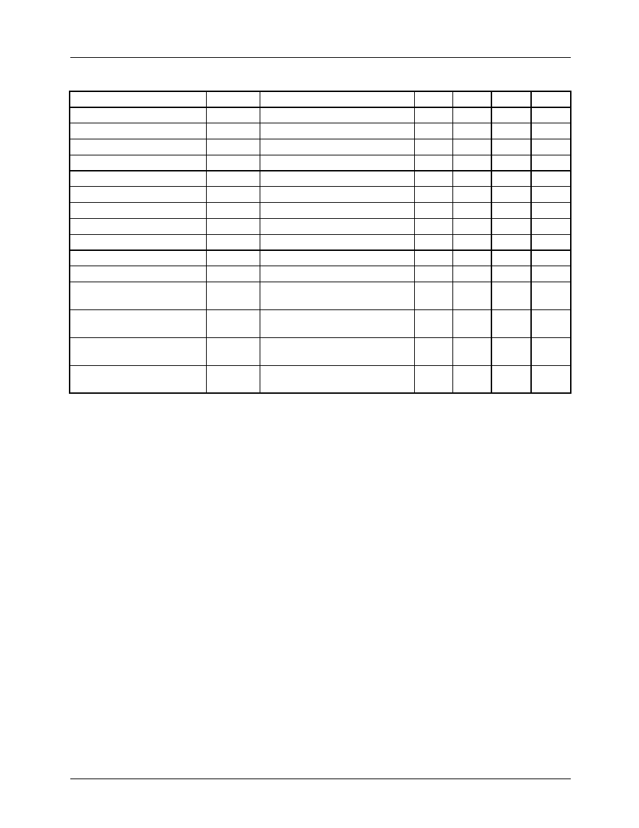
Electrical Characteristics (Ta=25
°
°
°
°
C, Vcc=12V)
Parameter
Symbol
Conditions
Min.
Typ.
Max.
Units
Quiescent current
I
Q
Pin5 & 6: GND, R
L
=
3
5.5
20
mA
Min. input-on current 1
I
IN1
R
L
=
, pin5=I
IN1
, pin6=L
-
10
50
µ
A
Min. input-on current 2
I
IN2
R
L
=
, pin5=L, pin6=I
IN2
-
10
50
µ
A
Input threshold voltage 1
V
INTH1
R
L
=
, pin5=V
INTH1
, pin6=L
0.7
1.3
2.0
V
Input threshold voltage 2
V
INTH2
R
L
=
, pin5=L, pin6=V
INTH2
0.7
1.3
2.0
V
Output leakage current 1
I
OL1
R
L
=
,
pin5 & 6=GND
-
-
1
mA
Output leakage current 2
I
OL2
R
L
=
,
pin5 & 6=GND
-
-
1
mA
Zener current 1
I
Z1
R
L
=
,
pin5=H, pin6=L
-
0.85
1.5
mA
Zener current 2
I
Z2
R
L
=
,
pin5=L, pin6=H
-
0.85
1.5
mA
Output voltage 1
V
O1
R
L
=60
,
pin5=H, pin6=L
6.6
7.2
-
V
Output voltage 2
V
O2
R
L
=60
,
pin5=L, pin6=H
6.6
7.1
-
V
Saturation voltage (Pin10-1)
V
CE10-1
R
L
=R
C
=
, pin5=H, pin6=L,
I
SINK
=100mA
-
0.83
1.5
V
Saturation voltage (Pin2-1)
V
CE2-1
R
L
=R
C
=
, pin5=L, pin6=H,
I
SINK
=100mA
-
0.83
1.5
V
Saturation voltage (Pin8-2)
V
CE8-2
R
L
=R
C
=
, pin5=H, pin6=L,
I
SOURCE
=100mA
-
0.83
1.5
V
Saturation voltage (Pin8-10)
V
CE8-10
R
L
=R
C
=
, pin5=L, pin6=H,
I
SOURCE
=100mA
-
0.83
1.5
V
KA8301
8
Application Information
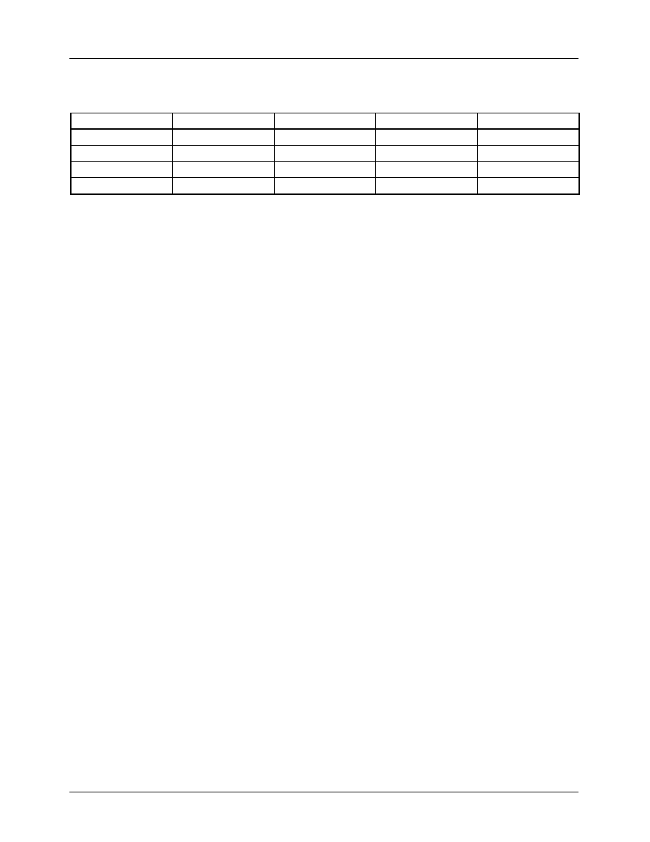
1. FORWARD AND REVERSE CONTROL LOGIC
· If pin #5=H, pin #6=L, load current flows from pin #2 to pin #10 through a motor.
· If pin #5=L, pin #6=H, load current flows from pin #10 to pin #2 through a motor.
· If pin #5=pin #6=L or pin #5=pin #6=H, the KA8301 stops supplying the power to motor while absorbing counter EMF
from the motor as a brake.
2. RUSH CURRENT RESTRICTING CIRCUIT
If a high voltage generated during reversing operation is applied across pin #2 and pin #10, an internal comparator activates
the rush current restricting circuit.
3. DRIVE CIRCUIT
In the forward mode, the drive circuit supplies a load current to the motor from pin #2 to pin #10.
In the reverse mode, it supplies the current from pin #10 to pin #2.
The output voltage (V
OUT
) applied to the motor is given by the followings;
V
OUT
= V
ZD
-
V
CE
(sat), where V
ZD
: a zener voltage applied to pin #4
If pin #4 is left open, the output voltage is given by the followings;
V
OUT
= V
CC1
-
V
CE
(sat, pnp)
-
2V
F
-
V
CE
(sat)
Pin #5
Pin #6
Pin #2
Pin #10
Function
L (0.7V
)
L (0.7V
)
L
L
Brake
L (0.7V
)
H (2.0V
)
L
H
Reverse
H (2.0V
)
L (0.7V
)
H
L
Forward
H (2.0V
)
H (2.0V
)
H
H
Brake
KA8301
9
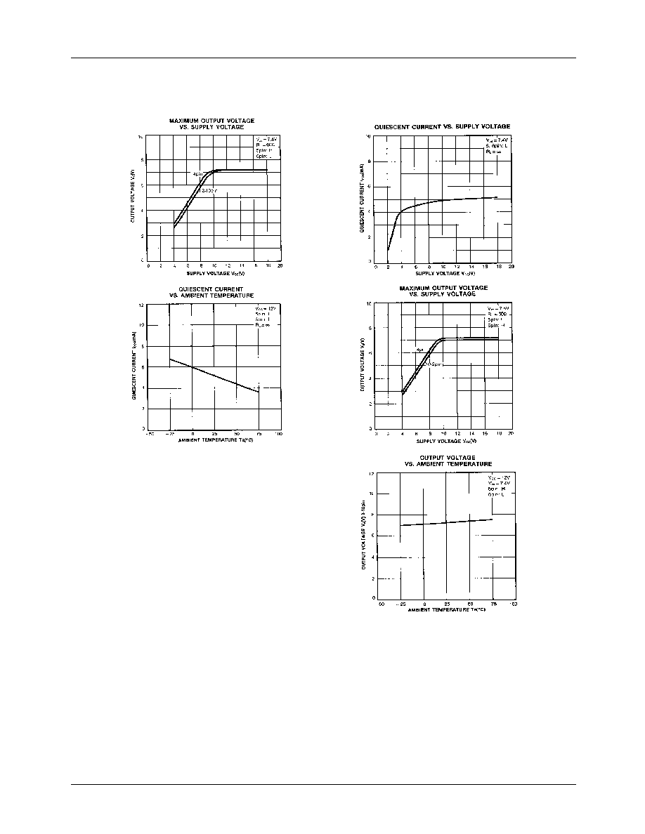
Typical Performance Characteristics
KA8301
10
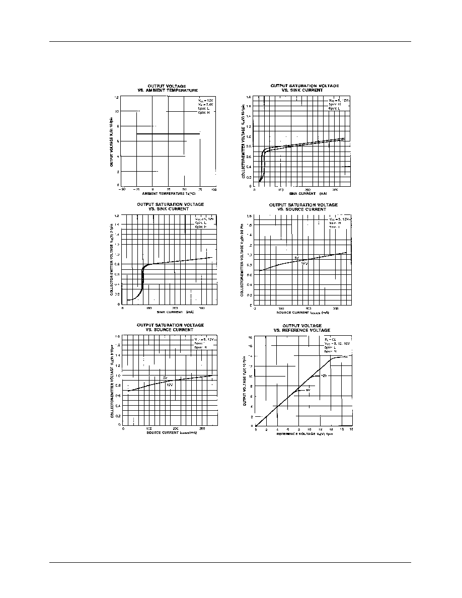
Typical Performance Characteristics (Continued)
KA8301
11
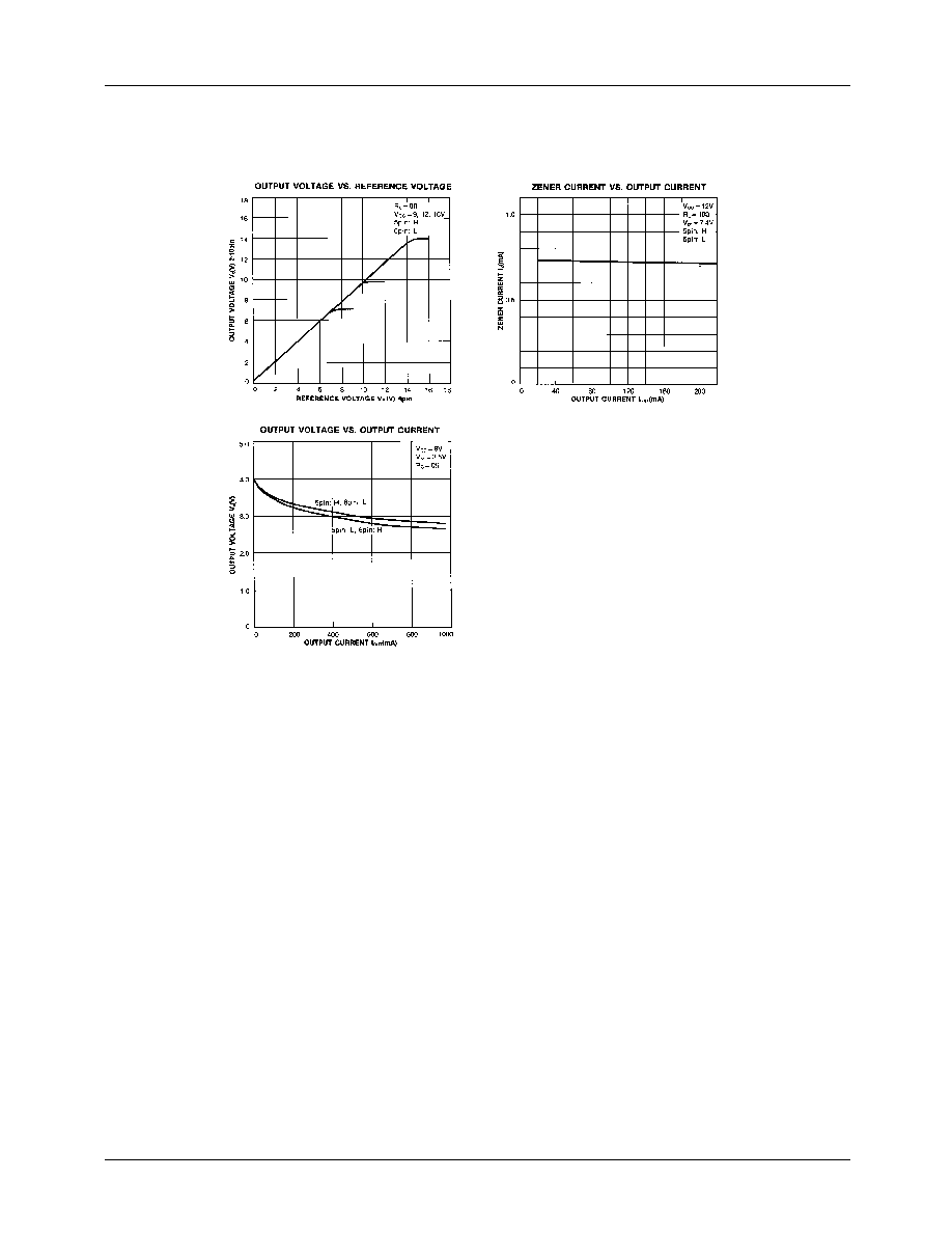
Typical Performance Characteristics (Continued)
KA8301
12
Test Circuits
Typical Application Circuits
1
2
3
4
5
6
7
8
9
10
KA8301
GND V
OUT1
V
Z1
V
R
F
IN
R
IN
V
CC1
V
CC2
V
Z2
V
OUT2
A
A
A
A
V
CC
S1
S2
Z
D
7.4V
V
IN
S5
S3
C
D
RC
S7
S4
10
0.1
µ
F
S6
9
10
KA8301
GND V
OUT1
V
Z1
V
R
F
IN
R
IN
V
CC1
V
CC2
V
Z2
V
OUT2
1
2
3
4
5
6
7
8
0.1
µ
10
V
CC
M

KA8301
12/1/00 0.0m 001
Stock#DSxxxxxxxx
2000 Fairchild Semiconductor International
LIFE SUPPORT POLICY
FAIRCHILD'S PRODUCTS ARE NOT AUTHORIZED FOR USE AS CRITICAL COMPONENTS IN LIFE SUPPORT DEVICES
OR SYSTEMS WITHOUT THE EXPRESS WRITTEN APPROVAL OF THE PRESIDENT OF FAIRCHILD SEMICONDUCTOR
INTERNATIONAL. As used herein:
1. Life support devices or systems are devices or systems
which, (a) are intended for surgical implant into the body,
or (b) support or sustain life, and (c) whose failure to
perform when properly used in accordance with
instructions for use provided in the labeling, can be
reasonably expected to result in a significant injury of the
user.
2. A critical component in any component of a life support
device or system whose failure to perform can be
reasonably expected to cause the failure of the life support
device or system, or to affect its safety or effectiveness.
www.fairchildsemi.com
DISCLAIMER
FAIRCHILD SEMICONDUCTOR RESERVES THE RIGHT TO MAKE CHANGES WITHOUT FURTHER NOTICE TO ANY
PRODUCTS HEREIN TO IMPROVE RELIABILITY, FUNCTION OR DESIGN. FAIRCHILD DOES NOT ASSUME ANY
LIABILITY ARISING OUT OF THE APPLICATION OR USE OF ANY PRODUCT OR CIRCUIT DESCRIBED HEREIN; NEITHER
DOES IT CONVEY ANY LICENSE UNDER ITS PATENT RIGHTS, NOR THE RIGHTS OF OTHERS.