 | ÐлекÑÑоннÑй компоненÑ: KH104 | СкаÑаÑÑ:  PDF PDF  ZIP ZIP |
Äîêóìåíòàöèÿ è îïèñàíèÿ www.docs.chipfind.ru
Features
s
-3dB bandwidth of 1.1GHz
s
325psec rise and fall times
s
14dB gain, 50
input and output
s
Low distortion, linear phase
s
1.4:1 VSWR (output, DC-1.1GHz)
s
Direct replacement for CLC104
Applications
s
Digital and wideband analog communications
s
Radar, IF and RF processors
s
Fiber optic drivers and receivers
s
Photomultiplier preamplifiers
General Description
The KH104 linear amplifier represents a significant
advance in linear amplifiers. Proprietary design
techniques have yielded an amplifier with 14dB of
gain and a -3dB bandwidth of DC to 1100MHz. Gain
flatness to 750MHz of ±0.4dB coupled with excellent
VSWR and phase linearity gives outstanding pulse
fidelity and low signal distortion.
Designed for 50
systems, the KH104 is very easy to
use, requiring only properly bypassed power supplies
for operation. This translates to time and cost savings
in all stages of design and production.
Fast rise time, low overshoot and linear phase make
the KH104 ideal for high speed pulse amplification.
These properties plus low distortion combine to
produce an amplifier well suited to many communi-
cations applications. With a 1.1GHz bandwidth, the
KH104 can handle the fastest digital traffic, even
when the demodulation scheme or the digital coding
format requires that DC be maintained. It is also
ideal for traditional video amplifier applications such
as radar or wideband analog communications systems.
These same characteristics make the KH104 an excellent
choice for use in fiber optics systems, on either the
transmitting or receiving end of the fiber. The low
group delay distortion insures that pulse integrity
will be maintained. As a photomultiplier tube pre-
amp, its fast response and quick overload recovery
provide for superior system performance.
The KH104 is constructed using thin film resistor/
bipolar transistor technology, and is available in the
following versions:
KH104AI
-25°C to +85°C
14-pin double-wide DIP
KH104
DC to 1.1GHz Linear Amplifier
www.fairchildsemi.com
REV. 1A February 2001
KH104
11 V
o
13 -V
R
14 +V
R
4
V
in
*
Ground
12
Offset
Adjust
+5.4V
Reg
1
+V
CC
-5.4V
Reg
2
*Pins 3, 5-10 case is ground
0.01
2.2
2.2
0.01
-15V
+15V
39
0.01
V
in
V
o
4
3,5-10
12
14
13
KH104
1
2
11
Capacitance if
µ
F
0.01
0.01
39
Offset
Adjust
10K
-15V
+15V
Basic Circuit Diagram
Equivalent Circuit Diagram
DATA SHEET
KH104
2
REV. 1A February 2001
PARAMETERS
CONDITIONS
TYP
MIN & MAX RATINGS
UNITS
SYM
Ambient Temperature
KH104AI
+25°C
Min
Max
FREQUENCY DOMAIN RESPONSE
-3dB bandwidth
0dBm out
1100
1000
MHz
SSBW
10dBm out
1050
MHz
SSBW
non-inverting gain (note 1)
@ 100MHz
14.2
13.8
14.9
dB
gain flatness
DC - 750MHz
±0.4
-0.6
+0.6
dB
linear phase deviation
DC - 600MHz
1.5
3
°
LPD
group delay
600
ps
GD
reverse isolation
DC - 750MHz
40
dB
RINI
750MHz - 1100MHz
35
dB
RIIN
input return loss
DC - 750MHz
18
dB
750MHz - 1100MHz
11
dB
output return loss
DC - 750MHz
17
dB
750MHz - 1100MHz
10
dB
TIME DOMAIN RESPONSE
rise and fall time
1V step
325
375
ps
TRS
(10% to 90%)
2V step
375
450
ps
TRL
settling time to 0.8%
1V step
1.2
ns
TS
overshoot
1V step
3
%
OS
overload recovery
V
inpeak
= ±0.5V
1.2
1.6
ns
OR
NOISE AND DISTORTION RESPONSE
2nd harmonic distortion
0dBm, 100MHz
47
-dBc
HD2
3rd harmonic distortion
0dBm, 100MHz
53
-dBc
HD3
2nd harmonic distortion
10dBm, 100MHz
40
30
-dBc
HD2
3rd harmonic distortion
10dBm, 100MHz
43
35
-dBc
HD3
3rd order intermolulation intercept
100MHz
26
+dBm
2-tone, 1MHz separation
500MHz
17
equivalent input noise voltage
10Hz to 1200MHz
55
dB
noise figure
11
dB
usable dynamic range
100MHz
71
dB
500MHz
65
dB
STATIC, DC PERFORMANCE
input bias current
note 2
80
280
µ
A
IBN
input bias current (drift)
note 2
0.6
2.0
µ
A/°C
IBN
output offset voltage
note 3
50
250
mV
output offset voltage (drift)
note 3
375
625
µ
V/°C
* supply current
no load
54
60
mA
ICC
supply rejection ratio
1KHz
55
dB
PSRR
Min/max ratings are based on product characterization and simulation. Individual parameters are tested as noted. Outgoing quality levels are
determined from tested parameters.
Absolute Maximum Ratings
Notes
V
CC
±9V to ±16V
I
o
±40mA
input voltage
±0.5V
junction temperature
+175°C
operating temperature
AI:
-25°C to +85°C
storage temperature
-65°C to +150°C
KH104 Electrical Characteristics
(T
A
= +25°C, V
CC
= ±15V, R
L
= 50
, R
s
= 50
; unless specified)
1. Nominal gain only - gain variation over temperature is ±0.1dB.
2. Input offset voltage = (input bias current) x (R
s
|| 50
).
3. Output offset can be adjusted to zero with an external
potentiometer see "Reducing DC Offset".
4. * AI 100% tested at 25°C.
AI Sample tested at 25°C.
KH104
DATA SHEET
REV. 1A February 2001
3
KH104 Performance Characteristics
(T
A
= +25°C, V
CC
= ±15V, R
L
= 50
, R
s
= 50
; unless specified)
Forward Gain and Phase
|S
21
| (dB)
16
14
8
Frequency (MHz)
0
260
520
780
1.04G
1.3G
12
10
S
21
S
21
(deg)
180
0
540
-180
-360
|S
21
|
P
o
= 0dBm
Reverse Gain and Phase
|S
12
| (-dB)
0
20
80
40
60
S
12
S
12
(deg)
360
180
-360
0
-180
|S
12
|
P
o
= 0dBm
Frequency (MHz)
0
260
520
780
1.04G
1.3G
Input Return Loss
|S
11
| (-dB)
0
20
80
40
60
Frequency (MHz)
0
260
520
780
1.04G
1.3G
Output Return Loss
|S
22
| (-dB)
0
20
80
40
60
Frequency (MHz)
0
260
520
780
1.04G
1.3G
Pulse Response
Input (40mV/div)
Output (200mV/div)
500ps/div
Input
Output
2nd and 3rd Harmonic Distortion
Distortion (dBc)
Frequency (Hz)
-20
-30
-80
100k
1M
10M
100M
1G
-40
-50
2nd
3rd
P
o
= 0dBm
-60
-70
2-Tone, 3rd Order Intermod. Intercept
Intercept Point (dBm)
Frequency (MHz)
30
25
0
0
200
400
600
1000
20
15
10
5
800
Noise Spectral Density
Noise Level (dBm/Hz)
Frequency (Hz)
-120
-170
10
1k
100k
1G
-130
-140
-150
-160
10M
-1dB Gain Compression
Power Output (dBm)
Frequency (MHz)
16
0
0
200
400
1000
12
8
4
600
800
Usable Dynamic Range
Dynamic Range (dB)
Frequency (MHz)
72
70
60
0
200
400
600
1000
68
66
64
62
800
Power Supply Rejection Ratio
PSRR (dB)
Frequency (Hz)
70
60
10
1
10
100
1k
1M
50
40
30
20
10k
100k
Relative Bandwidth vs. Case Temp.
Relative Bandwidth (%)
Case Temperature (
°
C)
105
100
80
0
20
40
60
140
95
90
85
80
100
120
P
d
= 1.6W
CA
= 30
°
C/W
DATA SHEET
KH104
4
REV. 1A February 2001
PC Board Layout Considerations
Proper layout of printed circuit boards is important to
achieve optimum performance of a circuit operating in the
1GHz frequency range. Use of microstripline is
recommended for all signal-carrying paths and low
resistance, low inductance signal return and bypass
paths should be used. To keep the impedance of
these paths low, use as much ground plane as possible.
Ground plane also serves to increase the flow of heat out
of the package.
The KH104 has three types of connections: signal paths
(input and output), DC inputs (supplies and offset adjust),
and grounds.
50
microstrip is recommended for
connection to the input (pin 4) and output (pin 11).
Microstrip on a doublesided PC board consists of a
ground plane on one side of the board and a constant-
width signal-carrying trace on the other side of the board.
For 1/16" G10 or FR-4 PC board material, a 0.1" wide
trace will have a 50
characteristic impedance.
The
ground plane beneath the signal trace must extend at
least one trace width on either side of the trace. Also, all
traces (including ground) should be kept at least one
trace width from the signal carrying traces.
To keep power supply noise and oscillations from appear-
ing at the amplifier output, all supply pins should be
capacitively bypassed to ground.
The power
supply pins (1 and 2) are the inputs to a pair of voltage
regulators whose outputs are at pins 13 and 14. It is
recommended that 0.01
µ
F or larger ceramic capacitors
be connected from pins 1, 2, 13 and 14 to ground, within
0.2" of the pins. A 1
µ
F or larger solid tantalum capacitor
to ground is required within 3" of pins 1 and 2, and
for good low frequency performance, solid tantalum
capacitors of at least 15
µ
F should be connected from
pins 13 and 14 to ground within 3" of the pins. Use 0.025"
or wider traces for the supply lines. The offset adjust pin
(12) also requires bypassing;
a 0.01
µ
F or
larger ceramic capacitor to ground within 0.2" of the pin is
recommended.
Grounding is the final layout consideration. Pins 3 and 5-
10 should all be connected to a ground plane which
should cover as much of one side of the board around the
amplifier as possible.
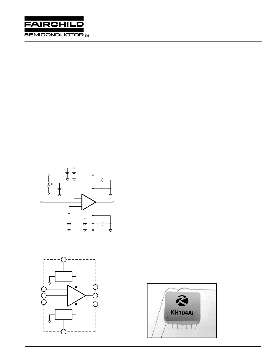
Reducing DC Offset
DC offset of the KH104 may be adjusted by applying a
DC voltage to the amplifier's offset adjust pin (12). The
simplest method is shown in Figure 1. Using this method
of offset adjust it is possible to vary the output offset by
approximately ±400mV. This simple adjustment has no
effect on the offset drift characteristics of the KH104.
Figure 1: Basic Circuit
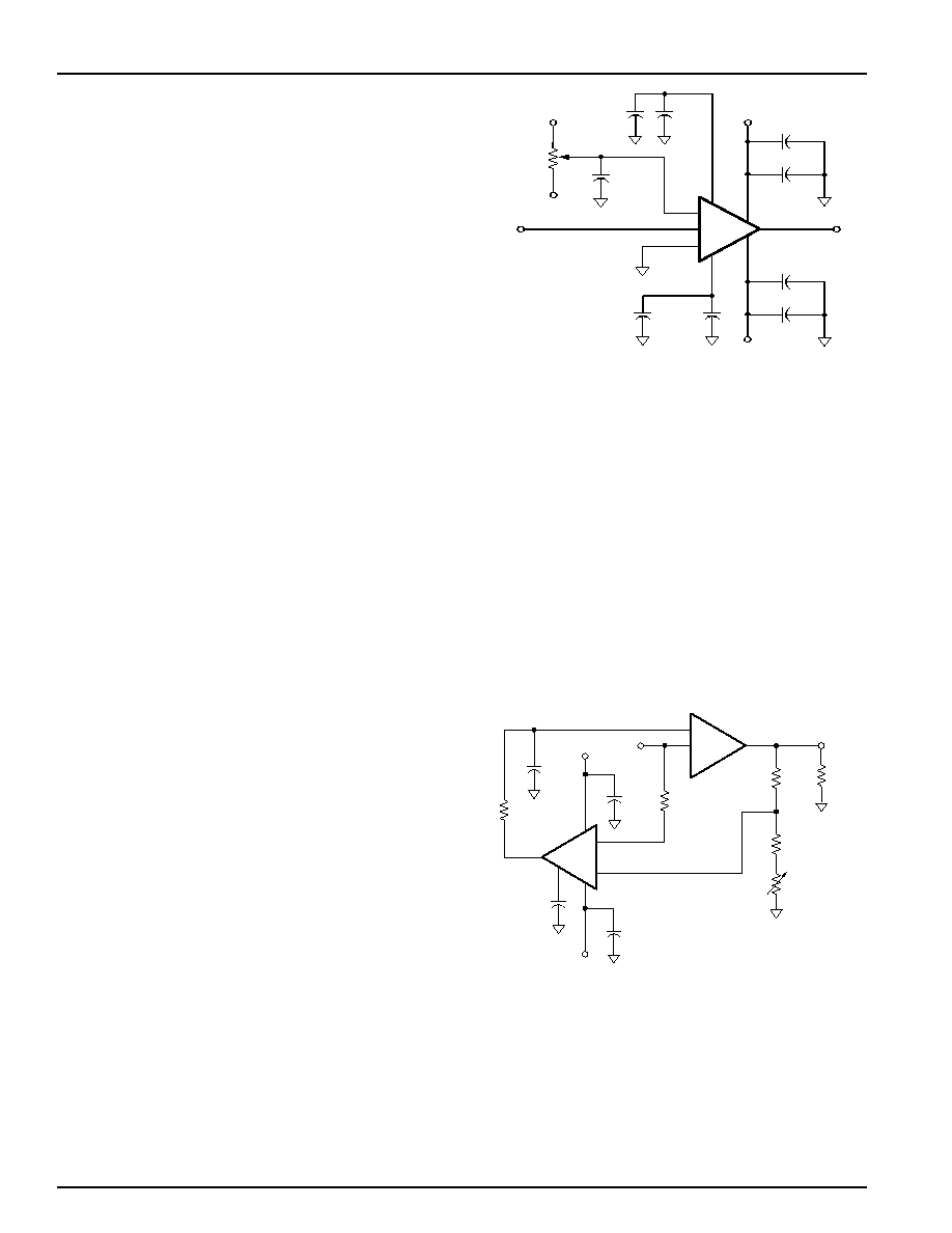
If lower offset and offset drift are required, a low frequency
op amp may be used in conjunction with the KH104 in a
composite configuration. The suggested circuit appears
in Figure 2. Its method of operation is to compare an
attenuated version of the output signal to the input signal
and apply a correcting voltage at the offset adjust pin. A
compensation capacitor C
s
reduces the bandwidth of the
op amp correction circuit to limit the op amp's effect on
the KH104 to frequencies below f
45
, the frequency at
which the op amp has 45dB of open loop gain. Using an
LM108, f
45
is about 7Hz with C
s
= 0.1
µ
F. Thus the op amp
can correct DC and low frequency errors below f
45
, with-
out affecting KH104 performance above f
45
. Also note
that the noise performance of the op amp will dominate
below f
45
.
Figure 2: Composite Amplifier
With an LM108 op amp in this composite configuration,
input offset is typically 2mV and drift is 15mV/°C.
At
frequencies well below f
45
, the composite gain is equal
to (1 + 49.9k/(R
a
+ R
b
)) and the output impedance is
0.01
2.2
2.2
0.01
-15V
+15V
39
0.01
V
in
V
o
4
3,5-10
12
14
13
KH104
1
2
11
Capacitance if
µ
F
0.01
0.01
39
Offset
Adjust
10K
-15V
+15V
V
in
V
o
4
12
KH104
LM108
0.01
0.01
2k
C
s
0.01
-15V
+15V
0.01
R
c
9.76k
6
7
8
4
2
3
11
49.9k
R
a
11.8k
R
b
1k
R
L
50
Capacitance in
µ
F
R
c
= (R
a
+ R
b
) || 49.9k
REV. 1A February 2001
5
KH104
DATA SHEET
voltage across the regulator of 3.6V and a minimum
regulator current of 10mA will satisfy the regulator
dropout voltage and current limits.
Given the maximum anticipated power supply voltages,
the shunt resistor should be calculated to yield a 35mA
current from that voltage to the regulated voltage of 5.4V.
This will leave 10mA through the regulator at the
minimum quiescent current of 45mA. The regulator input
voltages may be reduced directly by dropping the voltage
supplies, or, if that option is not available, using either
a zener or resistive dropping element in series with
the supply.
If a series dropping element is used, the
decoupling capacitors must appear on pins 1 and 2 of the
KH104. Figure 3 shows two possible power reduction
circuits from fixed ±15V supplies.
Several methods of decreasing the thermal resistance
from case to ambient are possible. With no heat paths
other than still air at 25°C, the thermal resistance from
case to ambient for the KH104 is about 40°C/W. When
placed in a printed circuit board with all ground pins
soldered into a ground plane 1" X 1.5", the thermal
resistance drops to about 30°C/W In this configuration,
the case rise will be 30°C for 9V supplies and 50°C
for 16V supplies.
This results in maximum allowable
ambient temperatures of 110°C and 90°C, respectively. If
higher operating temperatures are required, heat sinking
of the package is recommended.
Figure 3: Reducing Power Dissipation
very low. As the signal frequency increases beyond f
45
,
the op amp loses influence and the KH104 gain and
output impedance dominate. To ensure a smooth
transition and matched gain at all frequencies, adjust R
b
for a minimum op amp output swing with a 0.1V
pp
sinewave input (to the KH104) at the frequency f
45
. Since
the KH104 has a 50
output impedance, its
output voltage is a function of the load impedance
(A
v
~
_ 10R
L
/(R
L
+ 50)), whereas the gain of the compos-
ite amplifier at low frequencies and DC is relatively
independent of the load impedance, due to the high
open-loop gain of the op amp.
Thus, to avoid gain
mismatching and phase non-linearity, use the composite
amplifier only if the load impedance is constant from DC
to at least 10(f
45
).
Use of a composite amplifier reduces input offset voltage
and its corresponding drift, but has no effect on input bias
current. This current is converted to an input voltage by
the resistance to ground seen at the amplifier input and
the voltage appears, amplified, at the output.
Typical
input offset voltage due to the bias current is 2mV and
input offset drift is approximately 15mV/°C.
Thermal Considerations
The KH104 case must be maintained at or below 140°C.
Note that because of the amplifier design, power dissipa-
tion remains fairly constant, independent of the load or
drive level. Therefore, standard derating is not possible.
There are two ways to keep the case temperature low.
The first is to keep the amount of power dissipated inside
the package to a minimum and the second is to get the
heat out of the package quickly by reducing the thermal
resistance from case to ambient.
A large portion of the heat dissipated inside the package
is in the voltage regulators. At the minimum +9V supply
level the regulators dissipate 390mW and at the
maximum ±16V supply level they dissipate 1.2W.
The amplifier itself dissipates a fairly constant 600mW
(55mA x 10.8V). Reducing the power dissipation of the
internal regulators will go far towards reducing the
internal junction temperatures without impacting the so
performance. Reducing either the input supply voltages
(on pins 1 and 2) and/or shunting the regulator current
through external resistors (from pins 1 to 14 and pins
2 to 13) are both effective means towards significantly
reducing the internal power dissipation. A minimum
2.2
µ
F
0.01
µ
F
V
in
115
D1
5.6V
+15V
2.2
µ
F
0.01
µ
F
115
D2
5.6V
-15V
1
2
13
14
V
o
+
+
2.2
µ
F
0.01
µ
F
V
in
200
+15V
2.2
µ
F
0.01
µ
F
200
-15V
1
2
13
14
V
o
+
+
60
60
D1, D2 IN4734
nominal, no load P
d
~
760mW
nominal, no load P
d
~
900mW