 | ÐлекÑÑоннÑй компоненÑ: KH205AI | СкаÑаÑÑ:  PDF PDF  ZIP ZIP |
KH205 Overdrive-Protected Wideband Op Amp
Features
s
-3dB bandwidth of 170MHz
s
0.1% settling in 22ns
s
Complete overdrive protection
s
Low power: 570mW (190mW at ±5V)
s
3M
input resistance
s
Output may be current limited
s
Direct replacement for CLC205
Applications
s
Fast, precision A/D conversion
s
Automatic test equipment
s
Input/output amplifiers
s
Photodiode, CCD preamps
s
IF processors
s
High-speed modems, radios
s
Line drivers
General Description
The KH205 is a wideband overdrive-protected opera-
tional amplifier designed for applications needing
both speed and low power operation. Utilizing a
well-established current feedback architecture, the
KH205 exhibits performance far beyond that of
conventional voltage feedback op amps. For example,
the KH205 has a bandwidth of 170MHz at a gain of
+20 and settles to 0.1% in 22ns. Plus, the KH205 has
a combination of important features not found in
other high-speed op amps.
For example, the KH205 has been designed to consume
little power 570mW at ±15V supplies. The result is
lower power supply requirements and less system-
level heat dissipation. In addition, the device can be
operated on supply voltages as low as ±5V for even
lower power dissipation.
Complete overdrive protection has been designed
into the part. This is critical for applications, such as
ATE and instrumentation, which require protection
from signal levels high enough to cause saturation of
the amplifier. This feature allows the output of the
op amp to be protected against short circuits using
techniques developed for low-speed op amps. With
this capability, even the fastest signal sources can
feature effective short circuit protection.
The KH205 is constructed using thin film resistor/bipolar
transistor technology, and is available in the following
versions:
KH205AI
-25°C to +85°C
12-pin TO-8 can
KH205AK
-55°C to +125°C
12-pin TO-8 can, features
burn-in & hermetic testing
KH205AM
-55°C to +125°C
12-pin TO-8 can,
environmentally
screened and electrically
tested to MIL-STD-883
KH205HXC
-55°C to +125°C
SMD#: 5962-9083501HXC
KH205HXA
-55°C to +125°C
SMD#: 5962-9083501HXA
KH205
Overdrive-Protected Wideband Op Amp
www.fairchildsemi.com
REV. 1A February 2001
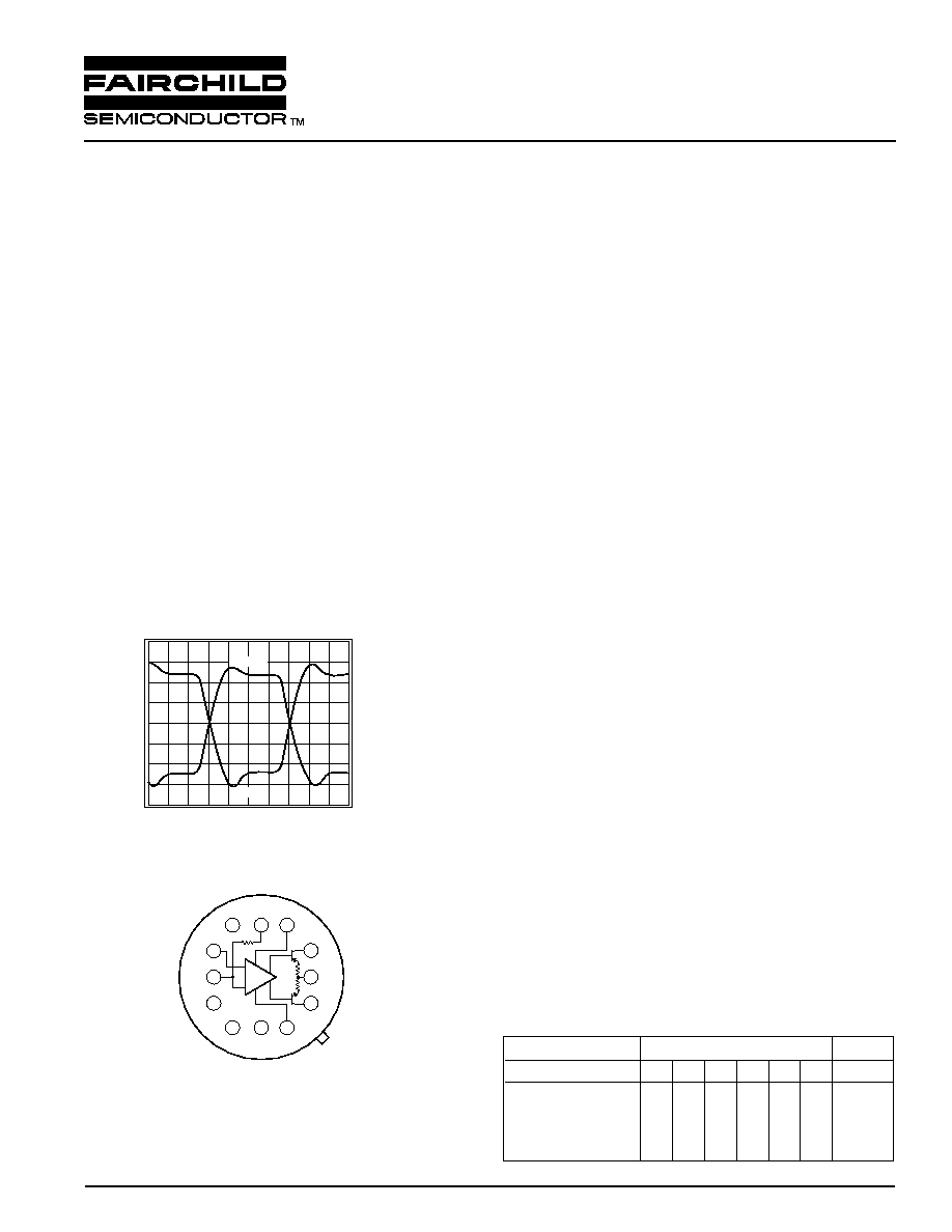
Large Signal Pulse Response
Output Voltage (2V/div)
Time (5ns/div)
A
v
= +20
A
v
= -20
Supply
Voltage
2000
8
R
f
7
GND
9
-V
CC
2
NC
3
GND
1
+V
CC
6
V+
5
V-
4
NC
10
-V
CC
V
o
+V
CC
11
12
6
6
Collector
Supply
Output
Collector
Supply
Supply
Voltage
Internal
Feedback
Not Connected
Case
ground
Non-Inverting
Input
Inverting
Input
Not
Connected
Case and
bias ground
+
-
Bottom View
Pin 8 provides access to a 2000
feed-
back resistor which can be connected to
the output or left open if an external feed-
back resistor is desired.
Typical Performance
Gain Setting
Parameter
+7
+20 +50
-1
-20 -50
Units
-3dB bandwidth
220 170
80 220 130 80
MHz
rise time
1.7
2.2
4.7 1.7
2.9 4.7
ns
slew rate
2.4
2.4
2.4 2.4
2.4 2.4
V/ns
settling time (to 0.1%)
22
22
20
21
20
19
ns

DATA SHEET
KH205
2
REV. 1A February 2001
PARAMETERS
CONDITIONS
TYP
MIN & MAX RATINGS
UNITS
SYM
Ambient Temperature
KH205AI
+25°C
-55°C
+25°C
+125°C
Ambient Temperature
KH205AK/AM/HXC/HXA
+25°C
-55°C +25°C
+125°C
FREQUENCY DOMAIN RESPONSE
-3dB bandwidth
V
o
= <2V
pp
170
>140
>140
>125
MHz
SSBW
large-signal bandwidth
V
o
= <10V
pp
100
>72
>80
>80
MHz
FPBW
gain flatness
V
o
= <2V
pp
peaking
0.1 to 35MHz
0
<0.3
<0.3
<0.5
dB
GFPL
peaking
>35MHz
0
<0.5
<0.5
<0.8
dB
GFPH
rolloff
at 70MHz
<0.8
<0.8
<0.8
dB
GFR
group delay
to 70MHz
3.0 ± .2
ns
GD
linear phase deviation
to 70MHz
0.8
<3.0
<2.0
<3.0
°
LPD
TIME DOMAIN RESPONSE
rise and fall time
2V step
2.2
<2.6
<2.6
<3.0
ns
TRS
10V step
4.8
<5.5
<5.5
<5.5
ns
TRL
settling time to 0.1%
10V step, note 2
22
<27
<27
<27
ns
TS
to 0.05%
10V step, note 2
24
<30
<30
<30
ns
TSP
overshoot
5V step
7
<14
<14
<14
%
OS
slew rate
20V
pp
at 50MHz
2.4
>1.8
>2.0
>2.0
V/ns
SR
NOISE AND DISTORTION RESPONSE
2nd harmonic distortion
2V
pp
, 20MHz
-57
<-50
<-50
<-50
dBc
HD2
3rd harmonic distortion
2V
pp
, 20MHz
-68
<-55
<-55
<-55
dBc
HD3
equivalent input noise
voltage
>100kHz
2.1
<3.0
<3.0
<3.5
nV/
Hz
VN
inverting current
>100kHz
22
<30
<30
<35
pA/
Hz
ICN
non-inverting current
>100kHz
4.8
<6.5
<6.5
<7.5
pA/
Hz
NCN
noise floor
>100kHz
-157
<-154
<-154
<-153
dBm(1Hz) SNF
integrated noise
1kHz to 150MHz
39
<55
<55
<61
µV
INV
noise floor
>5MHz
-157
<-154
<-154
<-153
dBm(1Hz) SNF
integrated noise
5MHz to 150MHz
39
<55
<55
<61
µV
INV
STATIC, DC PERFORMANCE
* input offset voltage
3.5
<8.0
<8.0
<11.0
mV
VIO
average temperature coefficient
11
<25
<25
<25
µV/°C
DVIO
* input bias current
non-inverting
3.0
<25
<15
<15
µ
IBN
average temperature coefficient
15
<100
<100
<100
nA/°C
DIBN
* input bias current
inverting
2.0
<22
<10
<25
µA
IBI
average temperature coefficient
20
<150
<150
<150
nA/°C
DIBI
* power supply rejection ratio
69
>55
>55
>55
dB
PSRR
common mode rejection ratio
60
>50
>50
>50
dB
CMRR
* supply current
no load
19
<20
<20
<22
mA
ICC
MISCELLANEOUS PERFORMANCE
non-inverting input resistance
DC
3.0
>1.0
>1.0
>1.0
M
RIN
non-inverting input capacitance
70MHz
5.0
<7.0
<7.0
<7.0
pF
CIN
output impedance
DC
<0.1
<0.1
<0.1
RO
output voltage range
no load
±12
>±11
>±11
>±11
V
VO
internal feedback resistor
absolute tolerance
<0.2
%
RFA
temperature coefficient
-100 ±40
ppm/°C
RFTC
inverting input current self limit
2.2
<3.0
<3.0
<3.2
mA
ICL
Min/max ratings are based on product characterization and simulation. Individual parameters are tested as noted. Outgoing quality levels are
determined from tested parameters.
Absolute Maximum Ratings
Recommended Operating Conditions
V
CC
±20V
V
CC
±5V to ±15V
I
o
±75mA
I
o
±50mA
common mode input voltage
±(|V
CC
| -1)V
common mode input voltage
±(|V
CC
| -5)V
differential input voltage
±3V
gain range
+7 to +50, -1 to -50
thermal resistance
(see thermal model)
operating temperature
AI: -25°C to +85°C
note 1:
* AI/AK/AM/HXC/HXA
100% tested at +25°C
AK/AM/HXC/HXA: -55°C to +125°C
AK/AM/HXC/HXA
100% tested at +25°C and
sample tested storage temperature
-65°C to +150°C
at -55°C and +125°C
lead temperature (soldering 10s)
+300°C
AI
sample tested at +25°C
note 2:
Settling time specifications require the use of an
external feedback resistor (2
)
KH205 Electrical Characteristics
(A
v
= +20V, V
CC
= ±15V, R
L
= 200
, R
f
= 2k
; unless specified)
KH205
DATA SHEET
REV. 1A February 2001
3
KH205 Typical Performance Characteristics
(T
A
= +25°C, A
v
= +20, V
CC
= ±15V, R
L
= 200
; unless specified)
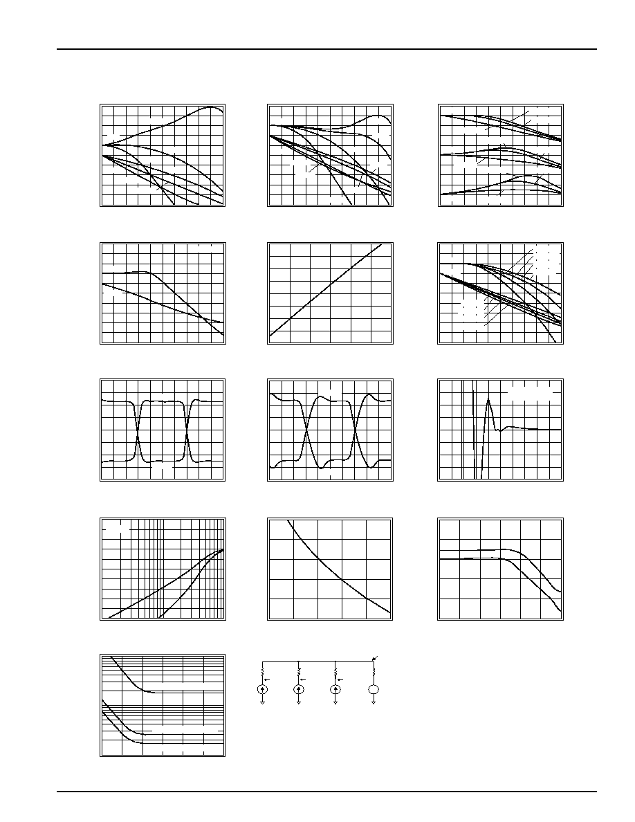
Non-Inverting Frequency Response
Normalized Magnitude (1dB/div)
Phase (45
°
/div)
Frequency (MHz)
0
20
40
60
80 100 120 140 160 180 200
Gain
Phase
A
v
= +7
A
v
= +20
A
v
= +50
A
v
= +7
A
v
= +20
A
v
= +50
Inverting Frequency Response
Normalized Magnitude (1dB/div)
Phase (45
°
/div)
Frequency (MHz)
0
20
40
60
80 100 120 140 160 180 200
Gain
Phase
A
v
= -1
A
v
= -7
A
v
= -1
A
v
= -7
A
v
= -20
A
v
= -50
A
v
= -20
A
v
= -50
Frequency Response vs. External R
f
Relative Gain (5dB/div)
Frequency (MHz)
0
20
40
60
80 100 120 140 160 180 200
R
f
= 1.5k
A
v
= +7
A
v
= +50
A
v
= +20
R
f
= 2k
R
f
= 3k
R
f
= 1.5k
R
f
= 2k
R
f
= 3k
R
f
= 1.5k
R
f
= 2k
R
f
= 3k
Large Signal Gain and Phase
Magnitude (1dB/div)
Phase (45
°
/div)
Frequency (MHz)
0
15
30
45
60
75
90 105 120 135 150
V
o
= 10V
pp
Gain
Phase
Relative Bandwidth vs. V
CC
Relative Bandwidth
±V
CC
(V)
4
6
8
10
12
14
16
0.2
0.3
0.4
0.5
0.6
0.7
0.8
0.9
1.0
Gain and Phase for Various Loads
Magnitude (1dB/div)
Phase (45
°
/div)
Frequency (MHz)
0
20
40
60
80 100 120 140 160 180 200
R
L
= 50
R
L
= 100
R
L
= 200
R
L
= 1k
R
L
= 1k
R
L
= 200
R
L
= 100
R
L
= 50
Gain
Phase
Small Signal Pulse Response
Output Voltage (0.4V/div)
Time (5ns/div)
A
v
= +20
A
v
= -20
Large Signal Pulse Response
Output Voltage (2V/div)
Time (5ns/div)
A
v
= +20
A
v
= -20
Settling Time
Settling Error (%)
Time (5ns/div)
10V step
R
f
= 2k
(external)
-0.20
-0.15
-0.10
-0.05
0
0.05
0.10
0.15
0.20
2nd and 3rd Harmonic Distortion
Distortion (dBc)
Frequency (MHz)
V
o
= 2V
pp
-80
-75
-70
-65
-60
-55
-50
-45
-40
-35
-30
1
10
100
2nd
3rd
2-Tone 3rd Order Intermodulation Intercept
Intercept (dBm)
Frequency (MHz)
20
25
30
35
40
45
0
20
100
40
60
80
CMRR and PSRR
PSRR and CMRR (dB)
Frequency (Hz)
0
20
40
60
80
100
100
1k
100M
10k
100k
1M
10M
PSRR
CMRR
Equivalent Input Noise
Noise Voltage (nV/
Hz)
Noise Current (pA/
Hz)
Frequency (Hz)
0
10
100
0
10
100
100
1k
100M
10k
100k
1M
100
Inverting Current 18.3 pA/
Hz
Non-Inverting Current 2.5 pA/
Hz
Voltage 1.8 nV/
Hz
Thermal Model
P
circuit
= [(+V
CC
) (-V
CC
)]
2
/ 1.77k
P
xxx
= [(±V
CC
) V
out
(I
col
) (R
col
+ 6)] (I
col
)
(% duty cycle)
(For positive V
o
and V
CC
, this is the power in the
npn output stage.)
(For negative V
o
and V
CC
, this is the power in the
pnp output stage.)
I
col
= V
out
/R
load
or 3mA, whichever is greater.
(Include feedback R in R
load
.)
R
col
is a resistor (33
recommended) between the
xxx collector and ±V
CC
.
T
j (pnp)
= P
pnp
(200 +
ca
) + (P
cir
+ P
npn
)
ca
+ T
a
,
similar for T
j (npn)
.
T
j (cir)
= P
cir
(17.5 +
ca
) + (P
pnp
+ P
npn
)
ca
+ T
a
.
+
-
T
ambient
ca
T
case
17.5
°
C/W
T
j(circuit)
P
circuit
200
°C/W
T
j(npn)
P
npn
200
°C/W
P
pnp
T
j(pnp)
DATA SHEET
KH205
4
REV. 1A February 2001
Current Feedback Amplifiers
Some of the key features of current feedback technology
are:
s
Independence of AC bandwidth and voltage gain
s
Adjustable frequency response with feedback resistor
s
High slew rate
s
Fast settling
Current feedback operation can be described using a simple
equation. The voltage gain for a non-inverting or inverting
current feedback amplifier is approximated by Equation 1.
Equation 1
where:
s
A
v
is the closed loop DC voltage gain
s
R
f
is the feedback resistor
s
Z(j
) is the CLC205's open loop transimpedance
gain
s
is the loop gain
The denominator of Equation 1 is approximately equal to
1 at low frequencies. Near the -3dB corner frequency, the
interaction between R
f
and Z(j
) dominates the circuit
performance. The value of the feedback resistor has a
large affect on the circuits performance. Increasing R
f
has the following affects:
s
Decreases loop gain
s
Decreases bandwidth
s
Reduces gain peaking
s
Lowers pulse response overshoot
s
Affects frequency response phase linearity
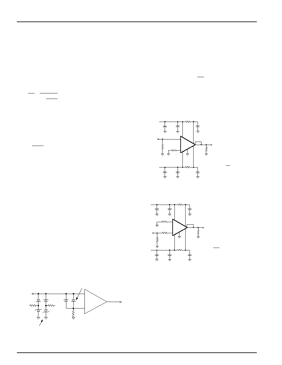
Overdrive Protection
Unlike most other high-speed op amps, the KH205 is not
damaged by saturation caused by overdriving input
signals (where V
in
x gain > max. V
o
). The KH205 self
limits the current at the inverting input when the output is
saturated (see the inverting input current self limit
specification); this ensures that the amplifier will not be
damaged due to excessive internal currents during overdrive.
For protection against input signals which would exceed
either the maximum differential or common mode input
voltage, the diode clamp circuits below may be used.
Figure 1: Diode Clamp Circuits for Common Mode
and Differential Mode Protection
Short Circuit Protection
Damage caused by short circuits at the output may be
prevented by limiting the output current to safe levels.
The most simple current limit circuit calls for placing
resistors between the output stage collector supplies and
the output stage collectors (pins 12 and 10). The value of
this resistor is determined by:
where I
I
is the desired limit current and R
I
is the minimum
expected load resistance (0
for a short to ground).
Bypass capacitors of 0.01
µF on should be used on the
collectors as in Figures 2 and 3.
Figure 2: Recommended Non-Inverting Gain Circuit
Figure 3: Recommended Inverting Gain Circuit
A more sophisticated current limit circuit which provides
a limit current independent of R
I
is shown in Figure 4 on
page 5.
With the component values indicated, current limiting
occurs at 50mA. For other values of current limit (I
I
),
select R
C
to equal V
be
/l
I
.
Where V
be
is the base to
emitter voltage drop of Q3 (or Q4) at a current of [2V
CC
1.4] / R
x
, where R
x
[(2V
CC
1.4) / I
I
] B
min
.
Also, B
min
is the minimum beta of Q1 (or Q2) at a current
of I
I
. Since the limit current depends on V
be
, which is
temperature dependent, the limit current is
likewise temperature dependent.
differential protection
KH205
+
-
common mode
protection
R
g
+V
cc
V
in
V
o
-V
cc
R
V
I
R
C
C
I
I
=
-
33
+15V
.1
3.9
.01
Capactance in
µF
1
12
8
3,7
200
10
11
33
.01
.1
3.9
-15V
9
+
-
KH205
V
o
R
f
= 2000
(internal)
6
V
in
5
R
i
50
R
g
A
1
R
R
v
f
g
= +
33
+15V
.1
3.9
.01
Capactance in
µF
1
12
8
5
V
in
3,7
200
10
R
i
11
33
.01
.1
3.9
-15V
9
+
-
KH205
V
o
R
f
= 2000
(internal)
6
50
R
g
For Z
in
= 50
, select R
g
||R
i
= 50
A
-R
R
v
f
g
=
V
V
A
1
R
Z j
o
in
v
f
=
+
( )
Z j
R
f
( )
KH205
DATA SHEET
REV. 1A February 2001
5
Figure 4: Active Current Limit Circuit (50mA)
Controlling Bandwidth and Passband Response
In most applications, a feedback resistor value of 2k
will provide optimum performance; nonetheless, some
applications may require a resistor of some other value.
The response versus R
f
plot on the previous page shows
how decreasing R
f
will increase bandwidth (and frequency
response peaking, which may lead to instability).
Conversely, large values of feedback resistance tend to
roll off the response.
The best settling time performance requires the use of an
external feedback resistor (use of the internal resistor
results in a 0.1% to 0.2% settling tail). The settling
performance may be improved slightly by adding a
capacitance of 0.4pF in parallel with the feedback
resistor (settling time specifications reflect performance
with an external feedback resistor but with no external
capacitance).
Noise Analysis
Approximate noise figure can be determined for the
KH205 using the Equivalent Input Noise plot on page 3
and the equations shown below.
kT = 4.00 x 10
-21
Joules at 290°K
V
n
is spot noise voltage (V/
Hz)
i
n
is non-inverting spot noise current (A/
Hz)
i
i
is inverting spot noise current (A/
Hz)
Figure 5: Noise Figure Diagram and Equations
(Noise Figure is for the Network Inside this Box.)
Driving Cables and Capacitive Loads
When driving cables, double termination is used to
prevent reflections. For capacitive load applications, a
small series resistor at the output of the KH205 will
improve stability and settling performance.
Transmission Line Matching
One method for matching the characteristic impedance
(Z
o
) of a transmission line or cable is to place the
appropriate resistor at the input or output of the amplifier.
Figure 6 shows typical inverting and non-inverting circuit
configurations for matching transmission lines.
Figure 6: Transmission Line Matching
Non-inverting gain applications:
s
Connect R
g
directly to ground.
s
Make R
1
, R
2
, R
6
, and R
7
equal to Z
o
.
s
Use R
3
to isolate the amplifier from reactive
loading caused by the transmission line,
or by parasitics.
Inverting gain applications:
s
Connect R
3
directly to ground.
s
Make the resistors R
4
, R
6
, and R
7
equal to Z
o
.
s
Make R
5
II R
g
= Z
o
.
The input and output matching resistors attenuate the
signal by a factor of 2, therefore additional gain is needed.
Use C
6
to match the output transmission line over a
greater frequency range. C
6
compensates for the increase
of the amplifier's output impedance with frequency.
Dynamic Range (Intermods)
For RF applications, the KH205 specifies a third
order intercept of 30dBm at 60MHz and P
o
= 10dBm.
A 2-Tone, 3rd Order IMD Intercept plot is found in
the Typical Performance Characteristics section.
The output power level is taken at the load. Third-order
harmonic distortion is calculated with the
formula:
HD3
rd
= 2
·
(IP3
o
P
o
)
R
s
R
n
R
o
R
f
R
g
KH205
+
-
F
R
R
R
kT
i
V
R
R
i
R
A
where R
R
R
R
R
A
R
R
s
n
s
n
n
p
f
i
p
v
p
s
n
s
n
v
f
g
=
+
+
+
+
=
+
=
+
10
1
4
1
2
2
2
2
2
2
2
log
;
Q3
(2N3906)
R
x
14.3k
Q4
(2N3904)
0.01
F
0.01
F
+V
cc
R
c
12
Q1
(MJE170)
Q2
(MJE180)
R
c
12
-V
cc
to pin 10
to pin 12
KH205
+
-
R
3
Z
0
R
6
V
o
Z
0
R
1
R
2
+
-
R
g
Z
0
R
4
R
5
V
1
V
2
+
-
R
f
C
6
R
7