 | ÐлекÑÑоннÑй компоненÑ: KH232AI | СкаÑаÑÑ:  PDF PDF  ZIP ZIP |
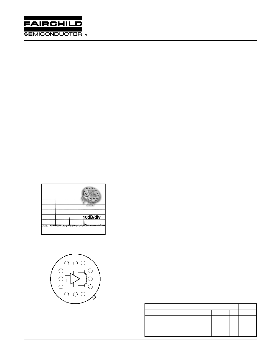
KH232 Low Distortion Wideband Op Amp
Features
s
-69dBc 2nd and 3rd harmonics at 20MHz
s
-3dB bandwidth of 270MHz
s
0.05% settling in 15ns
s
3000V/
µs slew rate
s
1mV input offset voltage, 10
µV/°C drift
s
±10V, 100mA max output
s
Direct replacement for CLC232
Applications
s
Flash A/D drivers
s
DAC current-to-voltage conversion
s
Wide dynamic range IF amps
s
VCO drivers
s
DDS postamps
s
Radar/communication receivers
s
Precision line drivers
General Description
The KH232 is a wideband low distortion operational
amplifier designed specifically for high speed, low gain
applications requiring wide dynamic range. Utilizing a
current feedback architecture, the KH232 offers high
speed performance while maintaining DC precision.
The KH232 offers precise gains from ±1 to ±5 with a
true 0.1% linearity and provides stable, oscillation-
free operation across the entire gain range without
external compensation. The KH232, a pin compatible
enhanced version of the KH231, reduces 2nd and 3rd
harmonic distortion to an extremely low -69dBc at
20MHz (2V
pp
, R
L
= 100
). Additional features provided
by the KH232 include a small signal bandwidth of
270MHz, a large signal bandwidth of 95MHz and a
3000V/
µs slew rate. The input offset voltage is typically
1mV with an input offset drift of 10
µV/°C.
The KH232 combines these high performance features
with its 0.05% settling time of 15ns and its 100mA
drive capability to provide high speed, high resolution
A/D and D/A converter systems with an attractive
solution for driving and buffering. Wide dynamic
range systems such as radar and communication
receivers requiring low harmonic distortion and low
noise will find the KH232 to be an excellent choice. As
a line driver, the KH232 set at a gain of 2 cancels
matched line losses.
The KH232 is constructed using thin film resistor/bipolar
transistor technology, and is available in the following
versions:
KH232AI
-25°C to +85°C
12-pin TO-8 can
KH232AK
-55°C to +125°C
12-pin TO-8 can, features
burn-in & hermetic testing
KH232AM
-55°C to +125°C
12-pin TO-8 can,
environmentally
screened and electrically
tested to MIL-STD-883
KH232HXC
-55°C to +125°C
SMD#: 5962-9166501HXC
KH232HXA
-55°C to +125°C
SMD#: 5962-9166501HXA
KH232
Low Distortion Wideband Op Amp
www.fairchildsemi.com
REV. 1A February 2001
Typical Performance
Gain Setting
Parameter
1
2
5
-1
-2
-5
Units
-3dB bandwidth
430 270 135 220 175 110
MHz
rise time (2V)
1.8
2.0
2.5
2.0
2.2
2.9
ns
slew rate
2.5
3.0
3.0
3.0
3.0
3.0
V/ns
settling time (to 0.1%)
12
12
12
12
12
15
ns
Supply
Voltage
8
Adjust
7
GND
9
-V
CC
2
Adjust
3
GND
1
+V
CC
6
V+
5
V-
4
NC
10
-V
CC
V
o
+V
CC
11
12
4
4
Collector
Supply
Output
Collector
Supply
Supply
Voltage
I
CC
Adjust
I
CC
Adjust
Case
ground
Non-Inverting
Input
Inverting
Input
Not
Connected
Case
ground
+
-
Bottom View
Pins 2 and 8 are used to adjust the sup-
ply current or to adjust the offset voltage
(see text). These pins are normally left
unconnected.

2
REV. 1A February 2001
DATA SHEET
KH232
PARAMETERS
CONDITIONS
TYP
MIN & MAX RATINGS
UNITS
SYM
Ambient Temperature
KH232AI
+25°C
-25°C
+25°C
+85°C
Ambient Temperature
KH232AK/AM/HXC/HXA
+25°C
-55°C
+25°C
+125°C
FREQUENCY DOMAIN RESPONSE
-3dB bandwidth (note 2)
V
o
0.63V
pp
270
>200
>200
>200
MHz
SSBW
V
o
2V
pp
165
>145
>145
>120
MHz
SSBW
large-signal bandwidth
V
o
10V
pp
95
>80
>80
>60
MHz
FPBW
gain flatness (note 2)
V
o
0.63V
pp
peaking
0.1 to 50MHz
0.1
<0.6
<0.3
<0.6
dB
GFPL
peaking
>50MHz
0.1
<1.5
<0.3
<0.8
dB
GFPH
rolloff
at 100MHz
0.4
<0.6
<0.6
<1.0
dB
GFR
group delay
to 100MHz
3.5 ± 0.5
ns
GD
linear phase deviation
to 100MHz
0.5
<2.0
<2.0
<2.0
°
LPD
reverse isolation
non-inverting
53
>43
>43
>43
dB
RINI
inverting
36
>26
>26
>26
dB
RIIN
TIME DOMAIN RESPONSE
rise and fall time
2V step
2.0
<2.4
<2.3
<2.7
ns
TRS
10V step
5.0
<7.0
<6.5
<6.5
ns
TRL
settling time to 0.05%
5V step
15
ns
TS
to 0.1%
2.5V step
12
<22
<17
<22
ns
TSP
overshoot
5V step
5
<15
<10
<15
%
OS
slew rate (overdriven input)
3.0
>2.5
>2.5
>1.8
V/ns
SR
overload recovery
<1% error
<50ns pulse, 200% overdrive
120
ns
OR
NOISE AND DISTORTION RESPONSE
2nd harmonic distortion
2V
pp
, 20MHz
-69
<-64
<-64
<-56
dBc
HD2
3rd harmonic distortion
2V
pp
, 20MHz
-69
<-64
<-64
<-64
dBc
HD3
equivalent input noise
voltage
>100kHz
2.8
<3.2
<3.2
<3.5
nV/
Hz
VN
inverting current
>100kHz
20
<23
<23
<25
pA/
Hz
ICN
non-inverting current
>100kHz
2.3
<2.6
<2.6
<2.9
pA/
Hz
NCN
noise floor
>100kHz
-155
<-154
<-154
<-153
dBm(1Hz)
SNF
integrated noise
1kHz to 200MHz
57
<64
<64
<72
µVrms
INV
integrated noise
5MHz to 200MHz
57
<64
<64
<72
µVrms
INV
STATIC, DC PERFORMANCE
* input offset voltage
1
<4.0
<2.0
<4.5
mV
VIO
average temperature coefficient
10
<25
<25
<25
µV/°C
DVIO
* input bias current
non-inverting
5.0
<29
<21
<31
µA
IBN
average temperature coefficient
50
<125
<125
<125
nA/°C
DIBN
* input bias current
inverting
10
<31
<15
< 35
µA
IBI
average temperature coefficient
125
<200
<200
<200
nA/°C
DIBI
* power supply rejection ratio
50
>45
>45
>45
dB
PSRR
common mode rejection ratio
46
>40
>40
>40
dB
CMRR
* supply current
no load
25
<27
<27
<29
mA
ICC
MISCELLANEOUS PERFORMANCE
non-inverting input resistance
DC
400
>100
>200
>400
k
RIN
non-inverting input capacitance
1.3
<2.5
<2.5
<2.5
pF
CIN
output impedance
@ 100MHz
5, 37
, nH
RO
output voltage range
no load
±12
>±11
>±11
>±11
V
VO
Min/max ratings are based on product characterization and simulation. Individual parameters are tested as noted. Outgoing quality levels are
determined from tested parameters.
Absolute Maximum Ratings
Recommended Operating Conditions
V
CC
±20V
V
CC
±5V to ±15V
I
o
±100mA
I
o
±75mA
common mode input voltage, V
o
|V
CC
| >15V ±(30-|V
CC
|)V
common mode input voltage
±(|V
CC
| -5)V
|V
CC
|
15V ±|V
CC
|V
gain range
±1 to ±5
differential input voltage
±3V
thermal resistance
(see thermal model)
junction temperature
+175°C
operating temperature
AI:
-25°C to +85°C
AK/AM/HXC/HXA: -55°C to +125°C
storage temperature
-65°C to +150°C
lead temperature (soldering 10s)
+300°C
KH232 Electrical Characteristics
(T
A
= +25°C, A
v
= +2V, V
CC
= ±15V, R
L
= 100
, R
f
= 250
; unless specified)
note 1:
* AI/AK/AM/HXC/HXA 100% tested at +25°C
AK/AM/HXC/HXA
100% tested at +25°C and sample
tested at -55°C and +125°C
AI
sample tested at +25°C
note 2:
The output amplitude used in testing is 0.63V
pp
. Performance
is guaranteed for conditions listed.
KH232
DATA SHEET
REV. 1A February 2001
3
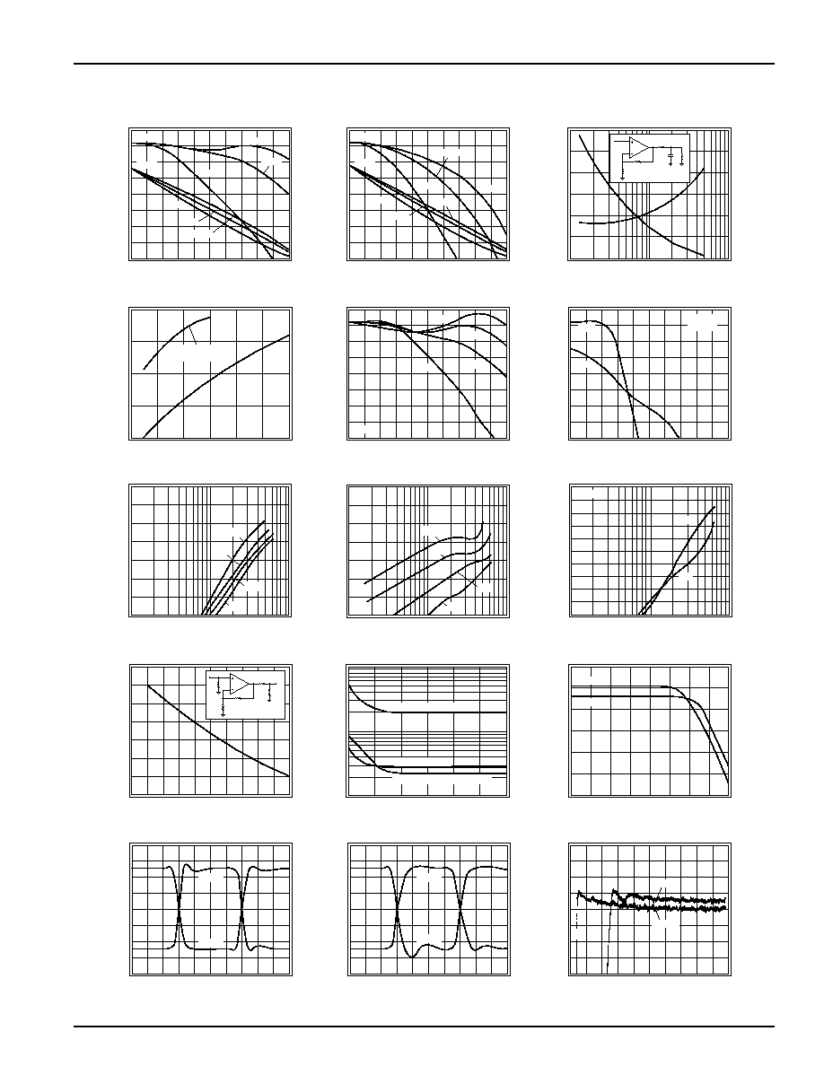
KH232 Typical Performance Characteristics
(T
A
= +25°C, A
v
= +2, V
CC
= ±15V, R
L
= 100
, R
f
= 250
; unless specified)
Non-Inverting Frequency Response
Normalized Magnitude (1dB/div)
Frequency (MHz)
0
150
300
Gain
Phase
Phase (45 deg/div)
A
v
= 5
A
v
= 1
A
v
= 2
A
v
= 5
A
v
= 2
A
v
= 1
Inverting Frequency Response
Normalized Magnitude (1dB/div)
Frequency (MHz)
0
150
300
Gain
Phase
Phase (45 deg/div)
A
v
= -5
A
v
= -1
A
v
= -2
A
v
= -5
A
v
= -2
A
v
= -1
Settling Time vs. C
L
Settling Time (ns)
C
L
(pF)
35
15
10
30
R
s
1k
5
0
100
1000
20
25
R
S
(
)
70
30
20
60
10
40
50
T
S
R
S
C
L
A
v
= +2
Bandwidth vs. V
CC
Relative Bandwidth
±V
CC
(V)
4
6
8
10
12
14
16
Pins 1 and 2 Shorted
Pins 8 and 9 shorted
0.4
0.6
0.8
1.0
1.2
Frequency Response vs. R
L
(1dB/div)
Frequency (MHz)
0
150
300
R
L
= 50
A
v
= 2
R
L
= 200
R
L
= 100
R
L
= 500
Large Signal Non-Inverting Gain & Phase
(1dB/div)
Phase (45 deg/div)
Frequency (MHz)
0
150
300
Gain
Phase
A
v
= 2
V
o
= 10V
pp
2nd Harmonic Distortion
Distortion (dBc)
Frequency (Hz)
1
10
100
-90
-60
-50
-40
-20
-30
4V
pp
-70
-80
8V
pp
2V
pp
1V
pp
3rd Harmonic Distortion
Distortion (dBc)
Frequency (Hz)
1
10
100
-90
-60
-50
-40
-20
-30
4V
pp
-70
-80
8V
pp
2V
pp
1V
pp
2nd and 3rd Harmonic Distortion
Distortion (dBc)
Frequency (MHz)
-40
-75
-70
-65
-60
-55
-50
-45
-90
1
10
100
-80
-85
2nd
3rd
V
o
= 2V
pp
2-Tone, 3rd Order Intermod. Intercept
Interdept Point (dBm)
Frequency (MHz)
50
35
25
20
45
50
50
P
out
15
0
10
20
30
40
50
60
70
80
90 100
30
40
Equivalent Input Noise
Noise Voltage (nV/
Hz)
Frequency (Hz)
100
10M
1k
10k
100k
1M
Inverting Current 20pA/
Hz
Non-Inverting Current 2.3pA/
Hz
Voltage 2.8nV/
Hz
1
10
100
Noise Current (pA/
Hz)
1
10
100
100M
CMRR and PSRR
CMRR
PSRR
PSRR/CMRR (dB)
Frequency (Hz)
1
10
100
1k
10k
100k
100M
10
30
40
50
1M
10M
20
Small Signal Pulse Response
Output Voltage (400mV/div)
Time (5ns/div)
A
v
= -2
A
v
= 2
Large Signal Pulse Response
Output Voltage (2V/div)
Time (5ns/div)
A
v
= -2
A
v
= 2
Settling Time
50ns/div
5ns/div
Settling Error (%)
Time (ns)
-0.20
-0.15
0.05
0.10
0.20
0.15
0
-0.05
-0.10
DATA SHEET
KH232
4
REV. 1A February 2001
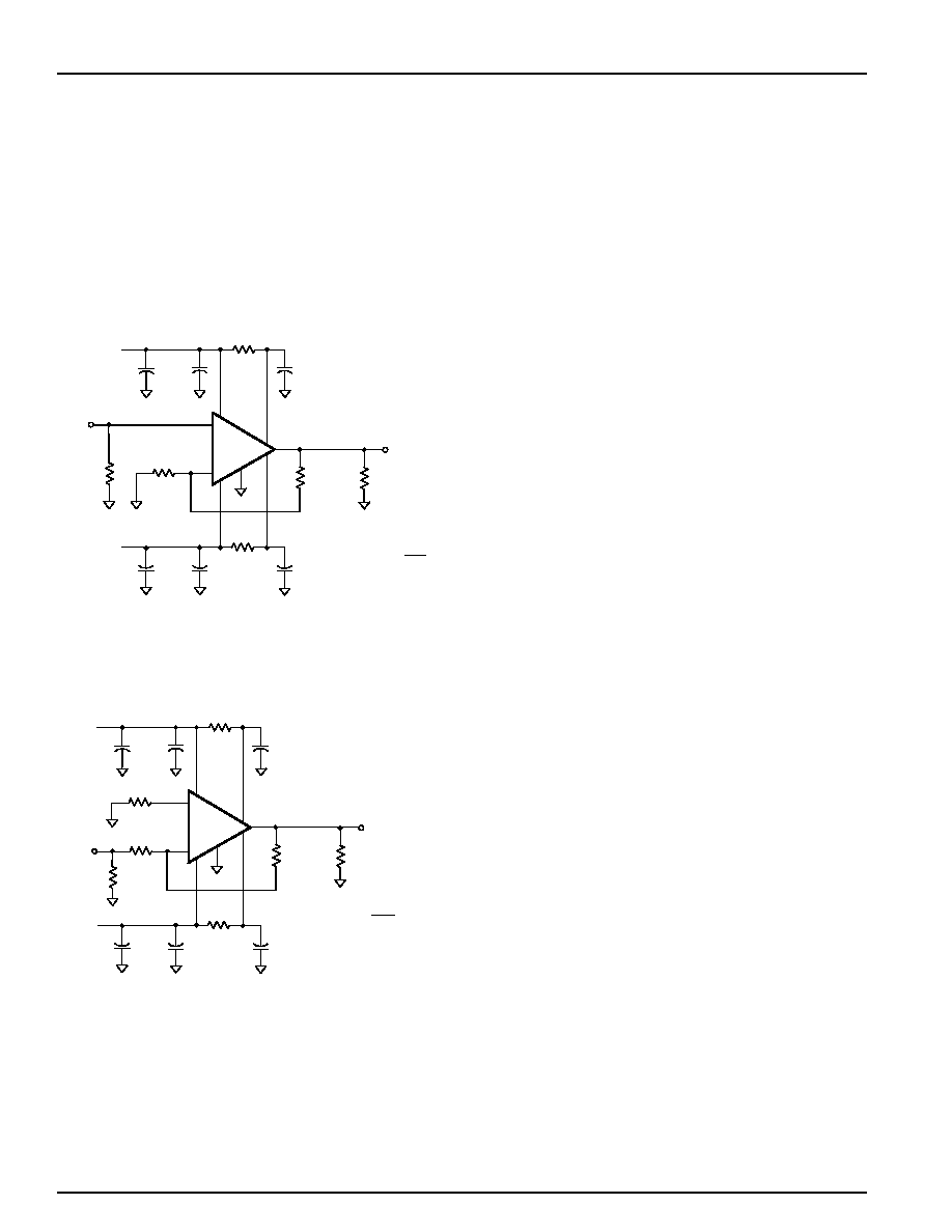
Operation
The KH232 is based on the current feedback op amp
topology, a design that uses current feedback instead of
the usual voltage feedback.
The use of the KH232 is basically the same as that of the
conventional op amp (see Figures 1 and 2). Since the
device is designed specifically for low gain applications,
the best performance is obtained when the circuit is used
at gains between ±1 and ±5. Additionally, performance is
optimum when a 250
feedback resistor is used.
Figure 1: Recommended non-inverting gain circuit
Figure 2: Recommended inverting gain circuit
Layout Considerations
To assure optimum performance the user should follow
good layout practices which minimize the unwanted
coupling of signals between nodes. During initial bread-
boarding of the circuit use direct point to point wiring,
keeping the lead lengths to less than 0.25". The use of
solid, unbroken ground plane is helpful. Avoid wire-wrap
type pc boards and methods. Sockets with small, short
pin receptacles may be used with minimal performance
degradation although their use is not recommended.
During pc board layout keep all traces short and direct
The resistive body of R
g
should be as close as possible
to pin 5 to minimize capacitance at that point. For the
same reason, remove ground plane from the vicinity of
pins 5 and 6. In other areas, use as much ground plane
as possible on one side of the board. It is especially
important to provide a ground return path for current from
the load resistor to the power supply bypass capacitors.
Ceramic capacitors of 0.01 to 0.1
µf (with short leads)
should be less than 0.15 inches from pins 1 and 9.
Larger tantalum capacitors should be placed within one
inch of these pins. V
CC
connections to pins 10 and 12
can be made directly from pins 9 and 1, but better supply
rejection and settling time are obtained if they are
separately bypassed as in figures 1 and 2. To prevent
signal distortion caused by reflections from impedance
mismatches, use terminated microstrip or coaxial cable
when the signal must traverse more than a few inches.
Since the pc board forms such an important part of the
circuit, much time can be saved if prototype boards of any
high frequency sections are built and tested early in the
design phase.
Evaluation boards designed for either
inverting or non-inverting gains are available.
Offset Voltage Adjustment
If trimming of the input offset voltage (V
os
= V
ni
-V
in
) is
desired, a resistor value of 10k
to 1M placed between
pins 8 and 9 will cause V
os
to become more negative by
8mV to 0.2mV respectively. Similarly, a resistor placed
between pins 1 and 2 will cause V
os
, to become more
positive.
Thermal Considerations
At high ambient temperatures or large internal power
dissipations, heat sinking is required to maintain
acceptable junction temperatures. Use the thermal
model on the previous page to determine junction
temperatures. Many styles of heat sinks are available for
TO-8 packages; the Thermalloy 2240 and 2268 are good
examples. Some heat sinks are the radial fin type which
cover the pc board and may interfere with external
components. An excellent solution to this problem is to
use surface mounted resistors and capacitors.
They
have a very low profile and actually improve high
frequency performance. For use of these heat sinks with
conventional components, a 0.1" high spacer can be inserted
under the TO-8 package to allow sufficient clearance.
33
+15V
0.1
3.9
.01
Capactance in
µF
1
12
5
3,7
R
L
100
10
11
33
.01
0.1
3.9
-15V
9
+
-
KH232
V
o
R
f
= 250
6
R
g
V
in
R
i
49.9
A
R
R
v
f
g
= 1+
250
33
+15V
0.1
3.9
.01
Capactance in
µF
1
12
5
3,7
R
L
100
10
11
33
.01
0.1
3.9
-15V
9
+
-
KH232
V
o
R
f
= 250
For Z
in
= 50
, select
R
g
|| R
i
= 50
6
100
V
in
R
i
250
R
g
A
R
R
v
f
g
= -
KH232
DATA SHEET
REV. 1A February 2001
5
Other methods of heat sinking may be used, but for
best results, make contact with the base of the KH232
package, use a large thermal capacity heat sink and use
forced air convection.
Low V
CC
Operation: Supply Current Adjustment
The KH232 is designed to operate on supplies as low
as ±5V. In order to improve full bandwidth at reduced
supply voltages, the supply current (I
CC
) must be
increased. The plot of Bandwidth vs. V
CC
, shows the
effect of shorting pins 1 and 2 and pins 8 and 9; this
will increase both bandwidth and supply current. Care
should be taken to not exceed the maximum junction
temperatures; for this reason this technique should not be
used with supplies exceeding ±10V. For intermediate val-
ues of V
CC
, external resistors between pins 1 and 2 and
pins 8 and 9 can be used.
P
(circuit)
= (I
CC
)((+V
CC
) (V
CC
)) where I
CC
= 14mA at ±15V
P
(xxx)
= [(±V
CC
) V
out
(I
col
) (R
col
+ 4)] (I
col
) (%Duty)
For positive V
o
and V
CC
, this is the power in the npn
device. For negative V
o
and V
CC
, this is the power in the
pnp device.
I
col
= V
o
/R
L
or 12mA, whichever is greater. (Include feed-
back R in R
L
.)
R
col
is a resistor (33
recommended) between the xxx
collector and ±V
CC
.
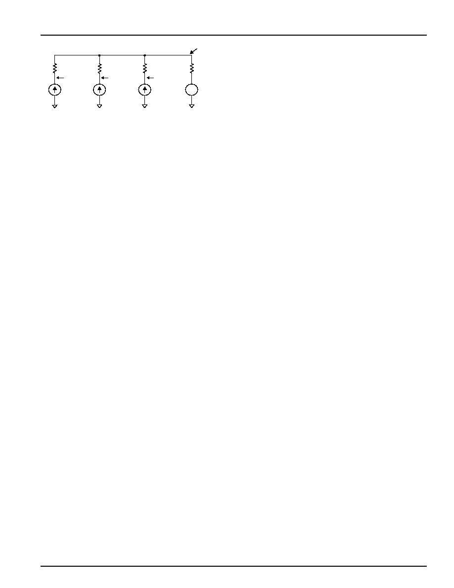
The limiting factor for output current and voltage is junction
temperature. Of secondary importance is I
(out)
, which
should not exceed 150mA.
T
j(pnp)
= P
(pnp)
(100 +
ca
) + (P
(cir)
+ P
(npn)
)(
ca
) + T
a
,
similar for T
j(npn)
.
T
j(cir)
= P
(cir)
(48 +
ca
) + (P
(pnp)
+ P
(npn)
)(
ca
) + T
a
.
ca
= 65°C/W for the KH232 without heat sink in still air.
35°C/W for the KH232 with a Thermalloy 2268A
heat sink in still air.
15°C/W for the KH232 with a Thermalloy 2268A
heat sink at 300 ft/min air.
(Thermalloy 2240A works equally as well.)
For example, with the KH232 operating at ±15V while
driving a 100
load at 15V
pp
output (50% duty cycle
pulse waveform, DC = 0), P
(npn)
= P
(pnp)
= 190mW (R
col
= 33) and P
(cir)
= 0.42W.
Then with the Thermalloy
2268 heat sink and air flow of 300 ft/min the output
transistors' T
j
is 31°C above ambient and worst case T
j
in
the rest of the circuit is 32°C above ambient. In still air,
however, the rise in T
j
is 47°C and 48°C, respectively.
With no heat sink, the rise in T
j
is 71°C and 72°C,
respectively! Under most conditions, HEAT SINKING IS
REQUIRED.
+
-
T
ambient
ca
T
case
48
°
C/W
T
j(circuit)
P
circuit
100
°C/W
T
j(npn)
P
npn
100
°C/W
P
pnp
T
j(pnp)