 | ÐлекÑÑоннÑй компоненÑ: KH560 | СкаÑаÑÑ:  PDF PDF  ZIP ZIP |
Äîêóìåíòàöèÿ è îïèñàíèÿ www.docs.chipfind.ru
Features
s
120MHz bandwidth at +24dBm output
s
Low distortion
(2nd/3rd: -60/-62dBc @ 20MHz and 10dBm)
s
Output short circuit protection
s
User-definable output impedance, gain,
and compensation
s
Internal current limiting
s
Direct replacement for CLC560
Applications
s
Output amplification
s
Arbitrary waveform generation
s
ATE systems
s
Cable/line driving
s
Function generators
s
SAW drivers
s
Flash A/D driving and testing
General Description
The KH560 is a wideband DC coupled, amplifier that
combines high output drive and low distortion. At
an output of +24dBm (10V
pp
into 50
), the -3dB
bandwidth is 120MHz. As illustrated in the table
below, distortion performance remains excellent
even when amplifying high-frequency signals to high
output power levels.
With the output current internally limited to 250mA,
the KH560 is fully protected against shorts to ground
and can, with the addition of a series limiting resistor
at the output, withstand shorts to the ±15V supplies.
The KH560 has been designed for maximum flexibility
in a wide variety of demanding applications. The
two resistors comprising the feedback network set
both the gain and the output impedance, without
requiring the series backmatch resistor needed by
most op amps. This allows driving into a matched
load without dropping half the voltage swing
through a series matching resistor. External compen-
sation allows user adjustment of the frequency
response. The KH560 is specified for both maximally
flat frequency response and 0% pulse overshoot
compensations.
The combination of wide bandwidth, high output
power, and low distortion, coupled with gain, output
impedance and frequency response flexibility, makes
the KH560 ideal for waveform generator applications.
Excellent stability driving capacitive loads yields
superior performance driving ADC's, long transmission
lines, and SAW devices. A companion part, the
KH561, offers higher full power bandwidth for
broadband sinusoidal applications.
The KH560 is constructed using thin film resistor/bipolar
transistor technology, and is available in the following
versions:
KH560AI
-25°C to +85°C
24-pin Ceramic DIP
KH560AK
-55°C to +125°C
24-pin Ceramic DIP,
features burn-in
and hermetic testing
KH560AM
-55°C to +125°C
24-pin Ceramic DIP,
environmentally screened
and electronically tested
to MIL-STD-883
KH560
Wideband, Low Distortion Driver Amplifier
www.fairchildsemi.com
REV. 1A February 2001
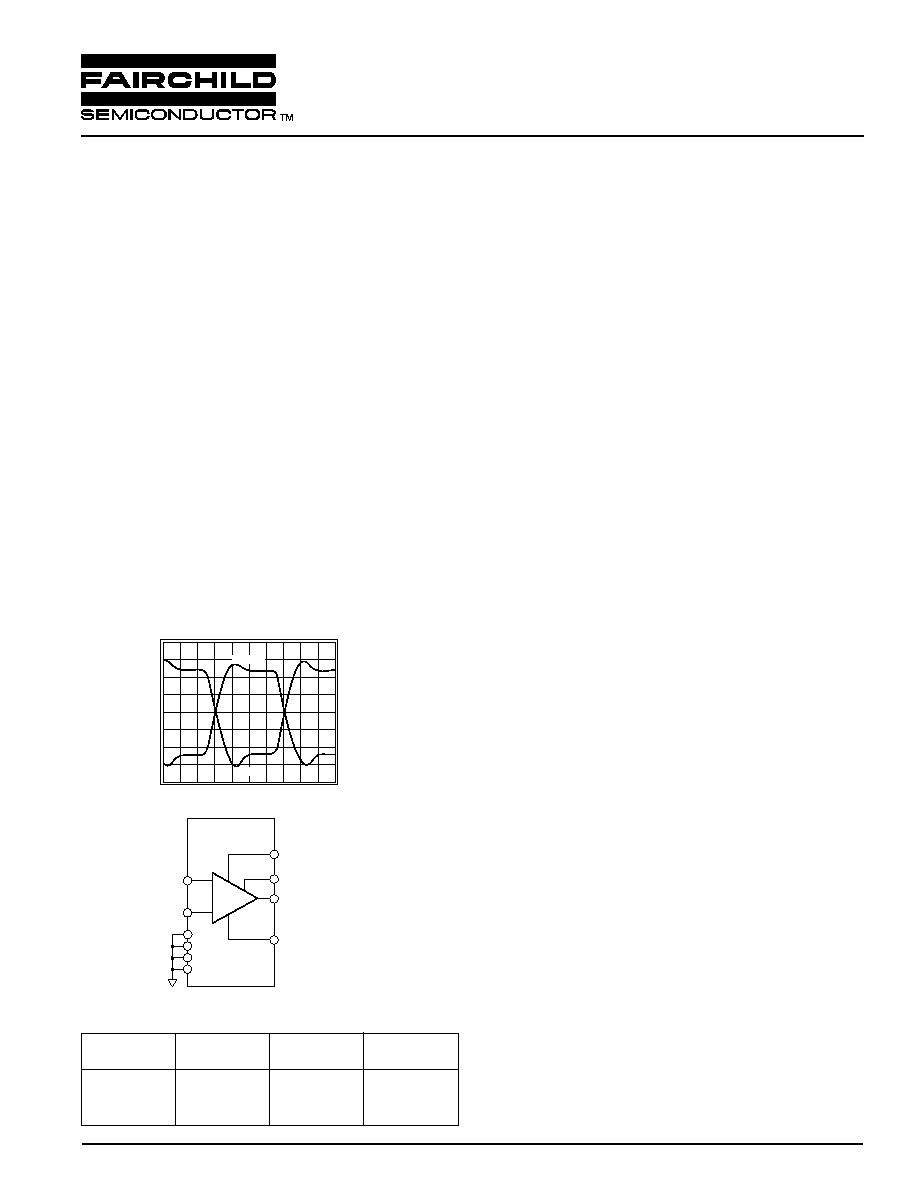
Large Signal Pulse Response
Output Voltage (2V/div)
Time (5ns/div)
A
v
= +20
A
v
= -20
Typical Distortion Performance
Output
20MHz
50MHz
100MHz
Power
2nd
3rd
2nd
3rd
2nd
3rd
10dBm
-60
-62
-50
-54
-54
-44
18dBm
-51
-48
-40
-40
-36
-29
24dBm
-46
-38
-33
-25
4
19
23
21
20
15
10
5
18
8
+
-
Compensation
V
o
-V
CC
All undesignated
pins are internally
unconnected. May
be grounded if
desired.
+V
CC
V+
V-
2
REV. 1A February 2001
DATA SHEET
KH560
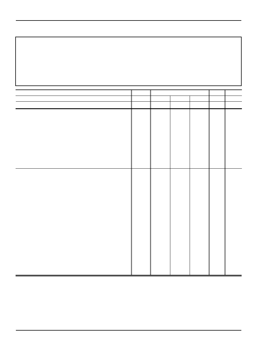
PARAMETERS
CONDITIONS
TYP
MIN & MAX RATINGS
UNITS
SYM
Case Temperature
KH560AI
+25°C
-25°C
+25°C
+85°C
Case Temperature
KH560AK/AM
+25°C
-55°C
+25°C
+125°C
FREQUENCY DOMAIN RESPONSE (Max. Flat Compensation)
-3dB bandwidth
maximally flat compensation
V
o
<2V
pp
(+10dBm)
215
>175
>185
>175
MHz
SSBW
0% overshoot compensation
V
o
<2V
pp
(+10dBm)
210
>170
>180
>170
MHz
large signal bandwidth
Vo <10V
pp
(+24dBm)
120
>115
>100
>90
MHz
FPBW
(see Frequency Response vs. Output Power plot)
gain flatness
V
o
<2V
pp
(+10dBm)
peaking
0.1 -50MHz
0
<0.50
<0.40
<0.50
dB
GFPL
peaking
>50MHz
0
<1.25
<0.75
<1.00
dB
GFPH
rolloff at
100MHz
0.1
<1.00
<0.75
<1.00
dB
GFR
group delay
to 100MHz
3.1
ns
GD
linear phase deviation
to 100MHz
0.6
<1.7
<1.2
<2.7
°
LPD
return loss (see discussion of R
x
)
to 100MHz
-15
<-12 <-12 <-12
dB RL
DISTORTION (Max. Flat Compensation)
2nd harmonic distortion
24dBm (10V
pp
):
20MHz
-46
<-36
<-36
<-33
dBc
HD2HL
50MHz
-33
<-27
<-27
<-27
dBc
HD2HM
18dBm (5V
pp
):
20MHz
-51
<-44
<-44
<-42
dBc
HD2ML
50MHz
-40
<-35
<-35
<-30
dBc
HD2MM
100MHz
-36
<-25
<-28
<-26
dBc
HD2MH
10dBm (2V
pp
):
20MHz
-60
<-54
<-54
<-50
dBc
HD2LL
50MHz
-50
<-43
<-43
<-40
dBc
HD2LM
100MHz
-54
<-32
<-32
<-32
dBc
HD2LH
3rd harmonic distortion
24dBm (10V
pp
):
20MHz
-38
<-32
<-32
<-25
dBc
HD3HL
50MHz
-25
<-21
<-21
<-20
dBc
HD3HM
18dBm (5V
pp
):
20MHz
-48
<-42
<-45
<-42
dBc
HD3ML
50MHz
-40
<-36
<-36
<-30
dBc
HD3MM
100MHz
-29
<-25
<-25
<-25
dBc
HD3MH
10dBm (2V
pp
):
20MHz
-62
<-58
<-58
<-57
dBc
HD3LL
50MHz
-54
<-50
<-50
<-48
dBc
HD3LM
100MHz
-44
<-40
<-40
<-36
dBc
HD3LH
2-tone 3rd order
intermod intercept
2
20MHz
40
>38
>38
>38
dBm
IM3L
50MHz
35
>32
>32
>32
dBm
IM3M
100MHZ
25
>23
>23
>20
dBm
IM3H
Min/max ratings are based on product characterization and simulation. Individual parameters are tested as noted. Outgoing quality levels are
determined from tested parameters.
KH560 Electrical Characteristics
(A
v
= +10V, V
CC
= ±15V, R
L
= 50
, R
f
= 410
, R
g
= 40
, R
o
= 50
; unless specified)
NOTES TO THE ELECTRICAL SPECIFICATIONS
The electrical characteristics shown here apply to the specific test conditions shown above (see also Figure 1 in
description of the operation). The KH560 provides an equivalent, non-zero, output impedance determined by the
external resistors. The signal gain to the load is therefore load dependent. The signal gain shown above (A
v
=
+10) is the no load gain. The actual gain to the matching 50
load used in these specifications is half of this (+5).
The KH560 requires an external compensation capacitor. Unless otherwise noted, this has been set to 10.5pF for
the frequency domain specifications (yielding a maximally flat frequency response) and 12.5pF for the time domain
specifications (yielding a 0% small signal pulse overshoot response).
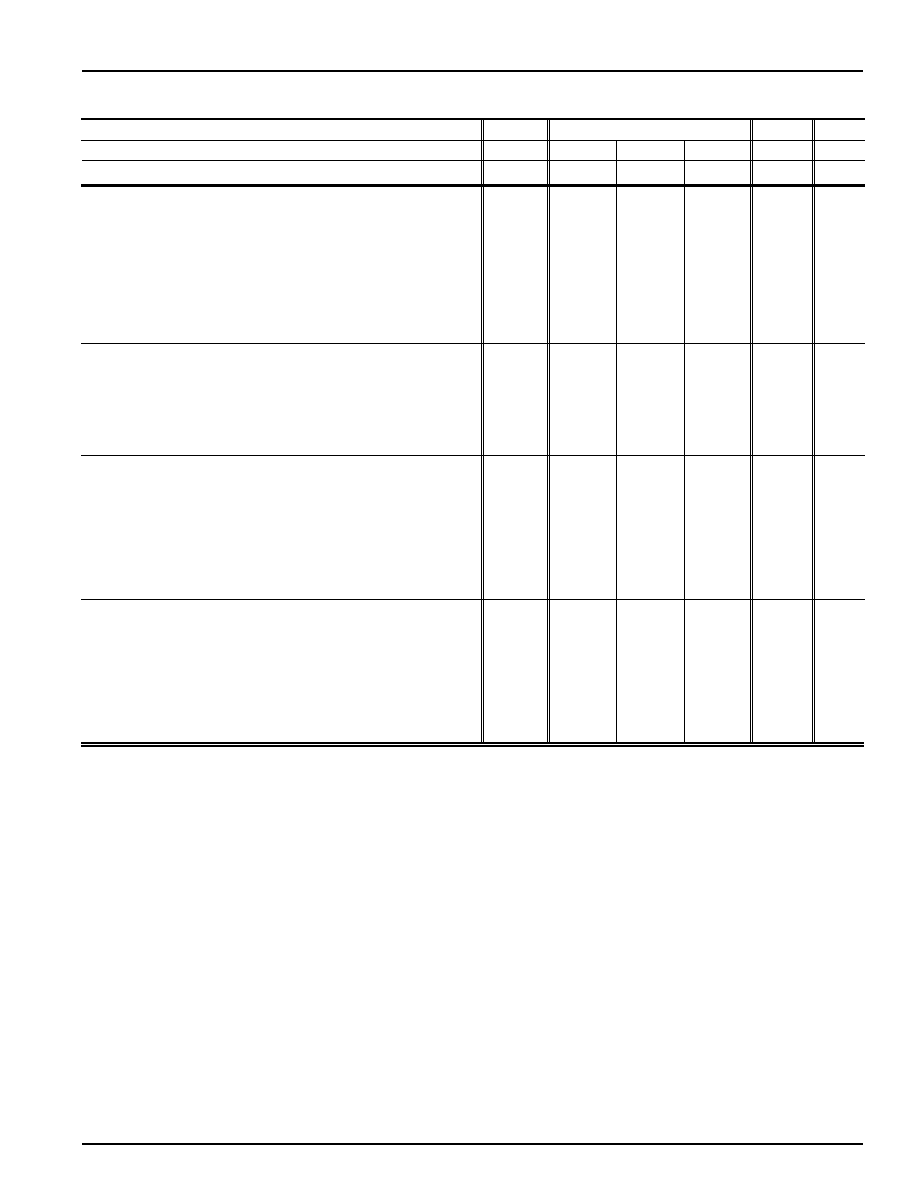
KH560
DATA SHEET
REV. 1A February 2001
3
PARAMETERS
CONDITIONS
TYP
MIN & MAX RATINGS
UNITS
SYM
Case Temperature
KH560AI
+25°C
-25°C +25°C
+85°C
Case Temperature
KH560AK/AM
+25°C
-55°C +25°C
+125°C
TIME DOMAIN RESPONSE (0% Overshoot Compensation)
rise and fall time
2V step
1.6
<2.0
<1.9
<2.0
ns
TRS
10V step
3.6
<3.8
<4.5
<5.3
ns
TRL
settling time to 0.1% (time <1
µs) 5V
step
10
<15
<15
<25
ns
TS
long term thermal tail (time >1
µs) 5V
step
0.4
<0.5
<0.5
<0.5
%
SE
slew rate
10V
pp
, 175MHz
2600
>2300
>2000
>1800
V/
µs
SR
overshoot
2V step
maximally flat compensation
5
<13
<10
<13
%
OSMF
0% overshoot compensation
0
<5
<3
<5
%
OSZO
EQUIVALENT INPUT NOISE
voltage
>100KHz
2.1
<2.5
<2.5
<2.5
nV/
Hz
VN
inverting current
>100KHz
34
<40
<40
<45
pA/
Hz
ICN
non-inverting current
>100KHz
2.8
<4.5
<4.5
<5.0
pA/
Hz
NCN
noise floor
3
>100KHz
-159
<-157 <-157 <-157
dBm/(1Hz)
SNF
integrated noise
3
1kHz to 200MHz
35
<45
<45 <45
µV
INV
noise figure
>100KHz
15
<17 <17 <17
dB
NF
STATIC, DC PERFORMANCE
* input offset voltage
2.0
<14.0 <5.0 <15.0
mV
VIO
average temperature coefficient
35
<100
<100
µV/°C
DVIO
* non-inverting bias current
5.0
<35
<20
<20
µA
IBN
average temperature coefficient
20
<175
<100
nA/°C
DIBN
* inverting bias current
10.0
<50
<30
<50
µA
IBI
average temperature coefficient
100
<200
<200
nA/°C
DIBI
* power supply rejection ratio (DC)
60
>58
>58
>57
dB
PSRR
* supply current
no load
50
<60
<60
<65
mA
ICC
MISCELLANEOUS PERFORMANCE
open loop current gain
(±1% tolerance)
10.0
mA/mA
G
average temperature coefficient
+0.02
<+.03
<+.02
%/°C
DG
inverting input resistance
(±5% tolerance)
14.0
RIN
average temperature coefficient
+.02
<+.025
<+.025
/°C
DRIN
non-inverting input resistance
700
>200
>400
>400
K
RNI
non-inverting input capacitance
to 100MHz
2.3
<3.0
<3.0
<3.0
pF
CNI
output voltage range
150mA load current
±10.5
>10.0
>10.0
>10.0
V
VO
output current limit
210
<250
<250
<250
mA
OCL
Min/max ratings are based on product characterization and simulation. Individual parameters are tested as noted. Outgoing quality levels are
determined from tested parameters.
Absolute Maximum Ratings
Recommended Operating Conditions
V
CC
(reversed supplies will destroy part)
±20V
V
CC
±10V to ±15V
differential input voltage
±3V
I
o
±200mA
common mode input voltage
±V
CC
common mode input voltage
< ±(|V
CC
| -6)V
junction temperature (see thermal model)
+175°C
output impedance
25
to 200
storage temperature
-65°C to +150°C
gain range (no-load voltage gain)
+5 to +80
lead temperature (soldering 10s)
+300°C
case temperature: AI
-25°C to +85°C
output current (internally limited)
±250mA
AK/AM
-55°C to +125°C
Notes
1) *
AI/AK/AM 100% tested at +25°C
AK/AM
100% tested at at +25°C and sample tested at -55°C and +125°C
AI
sample tested at +25°C
2) Test Tones are set ±100kHz of indicated frequency.
3) Noise tests are perfomed from 5MHz to 200MHz.
KH560 Electrical Characteristics
(A
v
= +10V, V
CC
= ±15V, R
L
= 50
, R
f
= 410
, R
g
= 40
, R
o
= 50
; unless specified)
DATA SHEET
KH560
4
REV. 1A February 2001
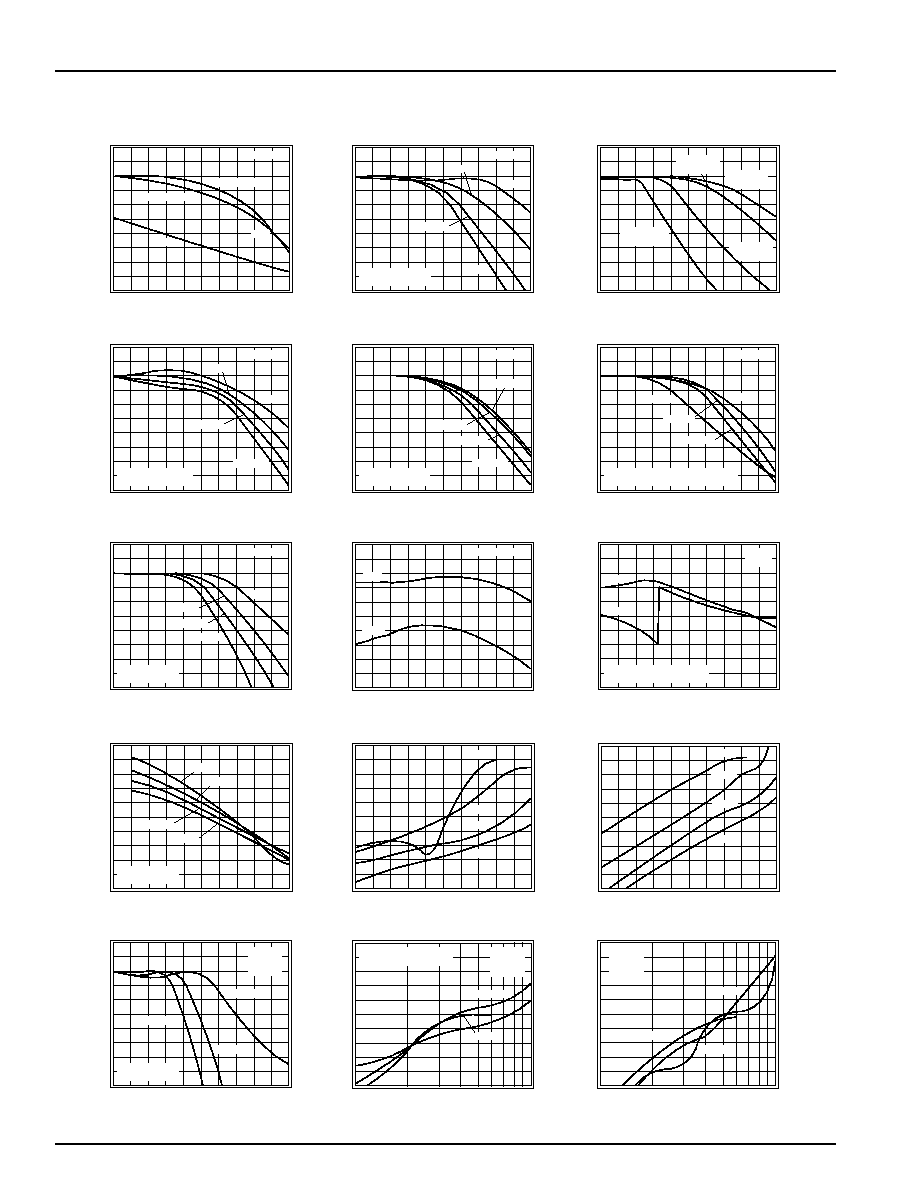
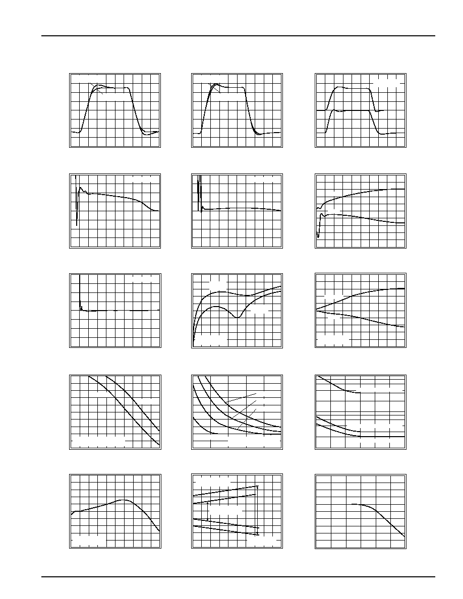
KH560 Typical Performance Characteristics
(T
A
= +25°C, Circuit in Figure 1; unless specified)
Small Signal Gain and Phase
Gain (dB)
Frequency (MHz)
6
8
10
12
14
16
0
50
100
150
200
250
Maximally Flat
Phase (degrees)
0
-90
-360
-180
-270
0% Overshoot
Gain
Phase
P
o
= 10dBm
Frequency Response vs. Gain
Normalized Magnitude (1dB/div)
Frequency (MHz)
0
50
100
150
200
250
P
o
= 10dBm
A
v
= 10
A
v
= 5
A
v
= 15
A
v
= 20
Re-compensated at
each gain (see text)
Frequency Response vs. Output Power
Gain (dB)
Frequency (MHz)
16
12
6
0
40
80
120
160
200
10
8
14
P
o
= 10dBm
V
o
= 2V
pp
P
o
= 24dBm
V
o
= 10V
pp
P
o
= 27.5dBm
V
o
= 15V
pp
P
o
= 18dBm
V
o
= 5V
pp
Frequency Response vs. R
L
Normalized Magnitude (1dB/div)
Frequency (MHz)
0
50
100
150
200
250
P
i
= -4dBm
R
L
= 50
R
L
= 25
R
L
= 75
R
L
= 100
Fixed gain and
compensated vs. load
Frequency Response vs. Power Supply
Frequency (MHz)
0
50
100
150
200
250
P
o
= 10dBm
±V
CC
= 18
±V
CC
= 12
±V
CC
= 15
±V
CC
= 10
Gain (dB)
16
12
6
10
8
14
Re-compensated at
each supply voltage
Frequency Response vs. R
o
Frequency (MHz)
0
50
100
150
200
250
P
i
= -4dBm
Normalized Magnitude (1dB/div)
R
o
= 50
R
o
= 25
R
o
= 75
R
o
= 100
Response measured with matched load
Re-compensated at each R
o
Frequency Response vs. Gain (R
o,
R
L
= 75
)
Frequency (MHz)
0
50
100
150
200
250
V
o
= 2V
pp
Normalized Magnitude (1dB/div)
A
v
= 5
A
v
= 10
A
v
= 15
A
v
= 20
Re-compensated
at each gain
Gain Flatness/Deviation from Linear Phase
Gain (0.1dB/div)
Frequency (MHz)
0
20
40
60
80
100
Phase (0.5
°
/div)
Gain
Phase
P
o
= 10dBm
Internal Current Gain and Phase
Gain (10dB/div)
Frequency (MHz)
-30
-20
0
20
30
10
0
100
200
300
400
500
Phase (90
°
/div)
180
90
-180
0
-90
Gain
Phase
-10
C
x
= 0
R
L
= 0
Phase consistant with current
polarity connection of Figure 3
Two Tone, 3rd-Order Intermodulation
Intercept (2.5dB/div)
Frequency (MHz)
45
35
20
0
20
40
60
80
100
30
25
40
A
v
= 15
A
v
= 5
A
v
= 10
A
v
= 20
Re-compensated
at each gain
2nd Harmonic Distortion vs. Frequency
Distortion (dBc)
Output Power (dB)
-25
-45
-75
4
8
12
16
20
24
-55
-65
-35
50MHz
10MHz
20MHz
100MHz
3rd Harmonic Distortion vs. Frequency
Distortion (dBc)
Output Power (dB)
-25
-45
-75
4
8
12
16
20
24
-55
-65
-35
50MHz
10MHz
20MHz
100MHz
Frequency Response Driving C
L
Frequency (MHz)
0
50
100
150
200
250
Gain (1dB/div)
A
v
= +5
R
o
= 25
V
o
= 2V
pp
C
L
= 100pF
C
L
= 20pF
C
L
= 50pF
Re-compensated
at each C
L
2nd Harmonic Distortion Driving C
L
Frequency (MHz)
10
20
30
40
50
100
Distortion (5dBc/div)
A
v
= +5
R
o
= 25
V
o
= 2V
pp
C
L
= 100pF
C
L
= 20pF
C
L
= 50pF
70
-80
-70
-60
-50
-40
-30
Compensation as shown in
Frequency Response plot
3rd Harmonic Distortion Driving C
L
Frequency (MHz)
10
20
30
40
50
100
Distortion (5dBc/div)
A
v
= +5
R
o
= 25
V
o
= 2V
pp
C
L
= 100pF
C
L
= 20pF
C
L
= 50pF
70
-80
-70
-60
-50
-40
-30
KH560
DATA SHEET
REV. 1A February 2001
5
KH560 Typical Performance Characteristics
(T
A
= +25°C, Circuit in Figure 1; unless specified)
Small Signal Pulse Response
Time (2ns/div)
Output Voltage (V)
Maximally Flat
Compensation
0
-1.2
-0.8
-0.4
0.4
1.2
0% Overshoot
Compensation
0.8
Large Signal Pulse Response
Time (5ns/div)
Output Voltage (V)
Maximally Flat
Compensation
0
-6
-4
-2
2
6
0% Overshoot
Compensation
4
Uni-Polar Pulse Response
Time (5ns/div)
Output Voltage (V)
Maximally Flat
Compensation
0
-6
-4
-2
2
6
4
Settling Time into 50
Load
Time (sec)
Settling Error (%)
0
-0.6
-0.4
-0.2
0.2
0.6
0.4
0.8
-0.8
10
-9
10
-7
10
-5
10
-3
10
-1
10
1
5V Output Step
Settling Time into 500
Load
Time (sec)
Settling Error (%)
5V Output Step
0
-0.6
-0.4
-0.2
0.2
0.6
0.4
0.8
-0.8
10
-9
10
-7
10
-5
10
-3
10
-1
10
1
Reverse Transmission Gain & Phase (S
12
)
Reverse Gain (dB)
Frequency (MHz)
-100
-80
-60
-40
-20
0
0
50
100
150
200
250
Reverse Phase (degrees)
0
-45
-180
-90
-135
Gain
Phase
Settling Time into 50pF Load
Time (sec)
Settling Error (%)
5V Output Step
0
-0.6
-0.4
-0.2
0.2
0.6
0.4
0.8
-0.8
10
-9
10
-7
10
-5
10
-3
10
-1
10
1
Output Return Loss (S
22
)
Magnitude (dB)
Frequency (MHz)
-25
-20
-15
-10
-5
0
0
50
100
150
200
250
R
o
= 50
R
x
= 0
-50
-45
-40
-35
-30
R
o
= 40
R
x
= 10
Re-compensated
at each R
x
Input Return Loss (S
11
)
Magnitude (dB)
Frequency (MHz)
-50
-40
-30
-20
-10
0
0
50
100
150
200
250
Phase (degrees)
0
-45
-180
-90
-135
Magnitude
Phase
Re-compensated
at each R
x
-1dB Compensation Point
-1dB Compensation (dBm)
Frequency (MHz)
27
28
29
30
31
32
0
20
40
60
80
100
R
o
= 50
22
23
24
25
26
R
o
= 75
Match Load
Re-compensated at each load
Noise Figure
Noise Figure (dBm)
No Load Gain
15
16
17
18
19
20
5
10
15
20
25
30
R
o
= 50
10
11
12
13
14
R
o
= 25
R
o
= 75
R
o
= 100
Non-inverting input impedance
matched to source impedance
Equivalent Input Noise
Noise Voltage (nV/
Hz)
Frequency (Hz)
1
6
20
40
60
100
100
1k
10k
100k
10M
100M
Inverting Current 34pA/
Hz
Noise Current (pA/
Hz)
10
4
2
1
6
20
40
60
100
10
4
2
Non-Inverting Voltage 2.1nV/
Hz
Non-Inverting Current 2.8pA/
Hz
1M
Group Delay
Group Delay (ns)
Frequency (MHz)
3.0
3.2
3.4
3.6
3.8
4.0
0
50
100
150
200
250
2.0
2.2
2.4
2.6
2.8
Aperture set to 5%
of span (12.8MHz)
Gain Error Band (Worst Case, DC)
Gain Error at Load (%)
No Load Gain
0
1
2
3
4
5
5
9
13
17
21
25
-5
-4
-3
-2
-1
R
o
(nominal) = 50
R
L
= 50
± 0%
R
f
and R
g
tolerance =
±0.1%
R
f
and R
g
tolerance =
±1%
PSRR
PSRR (dB)
Frequency (Hz)
50
60
70
80
90
100
100
1k
10k
100k
1M
100M
0
10
20
30
40
10M
Document Outline
- Main Menu
- Analog & Mixed Signal
- Analog Signal Processing
- High Performance Hybrid OpAmps
- Search
- fairchildsemi.com