Äîêóìåíòàöèÿ è îïèñàíèÿ www.docs.chipfind.ru
Features
s
505
µ
A supply current
s
75MHz bandwidth
s
Power down to Is = 33
µ
A (KM4120)
s
Fully specified at +2.7V and +5V supplies
s
Output voltage range: 0.07V to 4.86V; Vs = +5
s
Input voltage range: -0.3V to +3.8V; Vs = +5
s
50V/
µ
s slew rate
s
±15mA linear output current
s
±30mA output short circuit current
s
12nV/
Hz input voltage noise
s
Directly replaces AD8031 in single
supply applications
s
Small package options (SOT23-5 and SOT23-6)
Applications
s
Portable/battery-powered applications
s
A/D buffer
s
Active filters
s
Signal conditioning
s
Portable test instruments
General Description
The KM4110 (single) and KM4120 (single with disable)
are low cost, voltage feedback amplifiers. These
amplifiers are designed to operate on +2.7V, +5V, or
±2.5V supplies. The input voltage range extends
300mV below the negative rail and 1.2V below the
positive rail.
The KM4110 offers superior dynamic performance
with a 75MHz small signal bandwidth and 50V/
µ
s
slew rate. The combination of low power, high
output current drive, and rail-to-rail performance
make the KM4110 well suited for battery-powered
communication/ computing systems.
The combination of low cost and high performance
make the KM4110 suitable for high volume applica-
tions in both consumer and industrial applications
such as wireless phones, scanners, and color copiers.
KM4110/KM4120
0.5mA, Low Cost, +2.7V & +5V, 75MHz Rail-to-Rail Amplifiers
www.fairchildsemi.com
REV. 1A February 2001
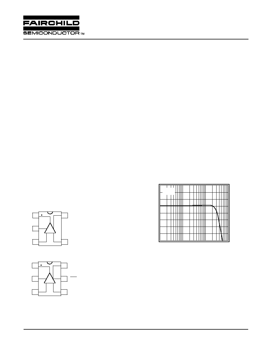
KM4110/KM4120 Packages
-
+
1
2
3
Out
-V
s
+In
+V
s
-In
5
4
-
+
1
2
3
Out
-V
s
+In
+V
s
-In
6
4
5
DIS
SOT23-5 (KM4110)
SOT23-6 (KM4120)
Non-Inverting Freq. Response V
s
= +5V
Normalized Magnitude (1dB/div)
Frequency (MHz)
0.1
1
10
100
G = 2
R
f
= 1k

DATA SHEET
KM4110/KM4120
2
REV. 1A February 2001
Parameters
Conditions
TYP
Min & Max
UNITS
NOTES
Case Temperature
+25°C
+25°C
Frequency Domain Response
-3dB bandwidth
G = +1, Vo = 0.05V
pp
65
MHz
1
G = +2, Vo < 0.2V
pp
30
MHz
full power bandwidth
G = +2, Vo = 2V
pp
12 MHz
gain bandwidth product
28
MHz
Time Domain Response
rise and fall time
0.2V step
7.5
ns
settling time to 0.1%
1V step
60
ns
overshoot
0.2V step,
10
%
slew rate
2.7V step
,
G = -1
40
V/
µ
s
Distortion and Noise Response
2nd harmonic distortion
1V
pp
, 1MHz
67
dBc
3rd harmonic distortion
1V
pp
, 1MHz
72
dBc
THD
1V
pp
, 1MHz
65
dB
input voltage noise
>1MHz
12
nV/
Hz
DC Performance
input offset voltage
0
±5
mV
2
average drift
10
µ
V/°C
input bias current
1.2
±3.5
µ
A
2
average drift
3.5
nA/°C
input offset current
30
350
nA
2
power supply rejection ratio
DC
66
60
dB
2
open loop gain
98
65
dB
2
quiescent current
470
600
µ
A
2
Disable Characteristics
turn on time
0.54
µ
s
turn off time
4.3
µ
s
off isolation
5MHz, RL = 100
58
dB
quiescent current
15
µ
A
Input Characteristics
input resistance
9
M
input capacitance
1.5
pF
input common mode voltage range
-0.3 to 1.5
V
common mode rejection ratio
DC, V
cm
= 0V to V
s
- 1.5
98
78
dB
2
Output Characteristics
output voltage swing
R
L
= 10k
to V
s
/2 0.05
to
2.6
V
R
L
= 1k
to V
s
/2
0.05 to 2.61
0.2 to 2.35
V
2
linear output current
±15
mA
short circuit output current
±25
mA
power supply operating range
2.7
2.5 to 5.5
V
Min/max ratings are based on product characterization and simulation. Individual parameters are tested as noted. Outgoing quality levels
are determined from tested parameters.
NOTES:
1) For G = +1, Rf = 0.
2) 100% tested at +25°C.
Absolute Maximum Ratings
Package Thermal Resistance
supply voltage
0 to +6V
Package
JA
maximum junction temperature
+175°C
5 lead SOT23
256°C/W
storage temperature range
-65°C to +150°C
6 lead SOT23
230°C/W
lead temperature (10 sec)
+300°C
operating temperature range (recommended) -40°C to +85°C
input voltage range
+V
s
+0.5V; -V
s
-0.5V
internal power dissipation
see power derating curves
KM4110/KM4120 Electrical Characteristics
(V
s
= +2.7V, G = 2, R
L
= 1k
to V
s
/2, R
f
= 1k
; unless noted)

KM4110/KM4120
DATA SHEET
REV. 1A February 2001
3
PARAMETERS
CONDITIONS
TYP
MIN & MAX
UNITS
NOTES
Case Temperature
+25°C
+25°C
Frequency Domain Response
-3dB bandwidth
G = +1, Vo = 0.05V
pp
75
MHz
1
G = +2, Vo < 0.2V
pp
35
MHz
full power bandwidth
G = +2, Vo = 2V
pp
15
MHz
gain bandwidth product
33
MHz
Time Domain Response
rise and fall time
0.2V step
6
ns
settling time to 0.1%
2V step
60
ns
overshoot
0.2V step,
12
%
slew rate
5V step
,
G = -1
50
V/
µ
s
Distortion and Noise Response
2nd harmonic distortion
2V
pp
, 1MHz
64
dBc
3rd harmonic distortion
2V
pp
, 1MHz
62
dBc
THD
2V
pp
, 1MHz
60
dB
input voltage noise
>1MHz
12
nV/
Hz
DC Performance
input offset voltage
-1
±5
mV
2
average drift
10
µ
V/°C
input bias current
1.2
±3.5
µ
A
2
average drift
3.5
nA/°C
input offset current
30
350
nA
2
power supply rejection ratio
DC
65
60
dB
2
open loop gain
80
65
dB
2
quiescent current
505
620
µ
A
2
Disable Characteristics
turn on time
0.33
µ
s
turn off time
5.5
µ
s
off isolation
5MHz, RL = 100
58
dB
quiescent current
33
µ
A
Input Characteristics
input resistance
9
M
input capacitance
1.5
pF
input common mode voltage range
-0.3 to 3.8
V
common mode rejection ratio
DC, V
cm
= 0V to V
s
- 1.5
92
78
dB
2
Output Characteristics
output voltage swing
R
L
= 10k
to V
s
/2
0.08 to 4.84
V
R
L
= 1k
to V
s
/2
0.07 to 4.86
0.2 to 4.65
V
2
linear output current
±15
mA
short circuit output current
±30
mA
power supply operating range
5
2.5 to 5.5
V
Min/max ratings are based on product characterization and simulation. Individual parameters are tested as noted. Outgoing quality levels
are determined from tested parameters.
NOTES:
1) For G = +1, Rf = 0.
2) 100% tested at +25°C.
KM4110/KM4120 Electrical Characteristics
(V
s
= +5V, G = 2, R
L
= 1k
to V
s
/2, R
f
= 1k
; unless noted)
DATA SHEET
KM4110/KM4120
4
REV. 1A February 2001
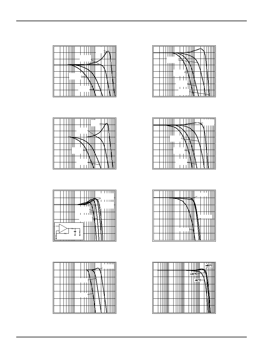
KM4110/KM4120 Performance Characteristics
(V
s
= +5V, G = 2, R
L
= 1k
to V
s
/2, R
f
= 1k
; unless noted)
Non-Inverting Freq. Response V
s
= +5V
Normalized Magnitude (1dB/div)
Frequency (MHz)
0.1
1
G = 10
R
f
= 1k
10
100
G = 5
R
f
= 1k
G = 1
R
f
= 0
G = 2
R
f
= 1k
Inverting Freq. Response V
s
= +5V
Normalized Magnitude (1dB/div)
Frequency (MHz)
0.1
1
G = -10
R
f
= 1k
10
100
G = -5
R
f
= 1k
G = -2
R
f
= 1k
G = -1
R
f
= 1k
Non-Inverting Freq. Response V
s
= +2.7V
Normalized Magnitude (2dB/div)
Frequency (MHz)
0.1
1
G = 10
R
f
= 2k
10
100
G = 5
R
f
= 1k
G = 1
R
f
= 0
G = 2
R
f
= 1k
Inverting Freq. Response V
s
= +2.7V
Normalized Magnitude (1dB/div)
Frequency (MHz)
0.1
1
G = -10
R
f
= 1k
10
100
G = -5
R
f
= 1k
G = -1
R
f
= 1k
G = -2
R
f
= 1k
Frequency Response vs. C
L
Magnitude (1dB/div)
Frequency (MHz)
0.1
1
10
100
C
L
= 100pF
R
s
= 100
C
L
= 50pF
R
s
= 100
C
L
= 10pF
R
s
= 0
C
L
= 20pF
R
s
= 100
+
-
1k
1k
R
s
C
L
R
L
Frequency Response vs. R
L
Magnitude (1dB/div)
Frequency (MHz)
0.1
1
10
100
R
L
= 1k
R
L
= 10k
R
L
= 100
Large Signal Frequency Response
Magnitude (1dB/div)
Frequency (MHz)
0.1
1
10
100
V
o
= 1V
pp
V
o
= 2V
pp
V
o
= 4V
pp
Frequency Response vs. Temperature
Magnitude (1dB/div)
Frequency (MHz)
0.01
1
100
10
0.1
REV. 1A February 2001
5
KM4110/KM4120
DATA SHEET
KM4110/KM4120 Performance Characteristics
(V
s
= +5V, G = 2, R
L
= 1k
to V
s
/2, R
f
= 1k
; unless noted)
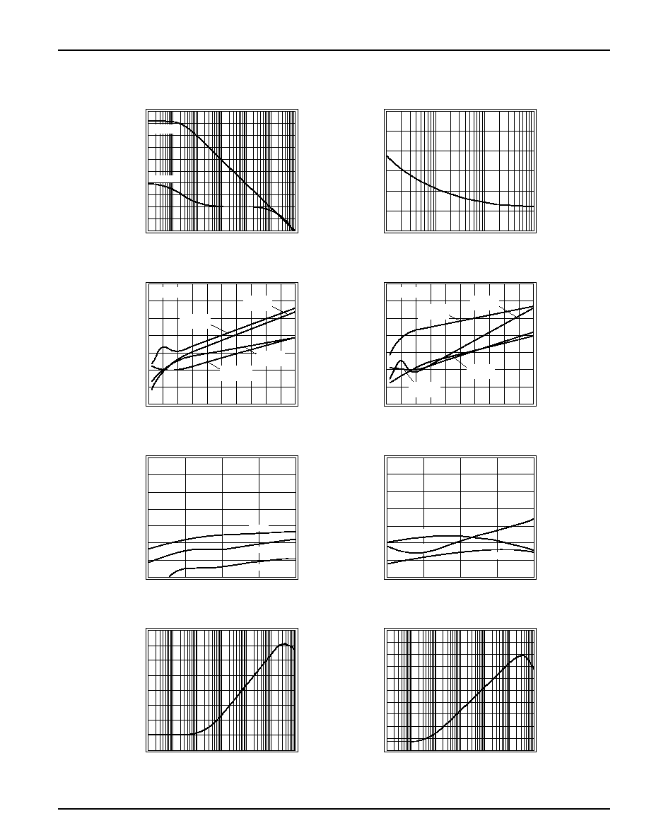
Open Loop Gain & Phase vs. Frequency
Open Loop Gain (dB)
Frequency (Hz)
-10
0
10
20
30
-180
-135
-90
-45
0
40
50
60
70
80
90
1k
100
10k
100k
1M
10M
100M
Open Loop Phase (deg)
|Gain|
Phase
Input Voltage Noise
Voltage Noise (nV/
Hz)
Frequency (Hz)
1k
10k
100k
1M
10
12
14
16
18
20
22
2nd & 3rd Harmonic Distortion; V
s
= +5V
Distortion (dBc)
Frequency (MHz)
0
1
2
3
4
3rd
R
L
= 1k
5
3rd
R
L
= 150
2nd
R
L
= 150
2nd
R
L
= 1k
-90
-80
-70
-60
-50
-40
-30
-20
V
o
= 2V
pp
2nd & 3rd Harmonic Distortion; V
s
= +2.7V
Distortion (dBc)
Frequency (MHz)
0
1
2
3
4
3rd
R
L
= 1k
5
3rd
R
L
= 150
2nd
R
L
= 150
2nd
R
L
= 1k
-90
-80
-70
-60
-50
-40
-30
-20
V
o
= 1V
pp
2nd Harmonic Distortion vs. V
o
Distortion (dBc)
Output Amplitude (V
pp
)
0.5
1
1.5
2
1MHz
500kHz
100kHz
2.5
-90
-80
-70
-60
-50
-40
-30
-20
3rd Harmonic Distortion vs. V
o
Distortion (dB)
Output Amplitude (V
pp
)
0.5
1.0
1.5
2.0
1MHz
500kHz
100kHz
2.5
-90
-80
-70
-60
-50
-40
-30
-20
PSRR
PSRR (dB)
Frequency (Hz)
100
1k
10k
10M
1M
100k
100M
-80
-70
-60
-50
-40
0
-30
-20
-10
CMRR
CMRR (dB)
Frequency (Hz)
100
1k
10k
10M
1M
100k
100M
-100
-90
-80
-70
-60
0
-50
-40
-10
-30
-20