 | ÐлекÑÑоннÑй компоненÑ: KM4200 | СкаÑаÑÑ:  PDF PDF  ZIP ZIP |
Äîêóìåíòàöèÿ è îïèñàíèÿ www.docs.chipfind.ru
-
+
-
+
1
2
3
4
Out1
-In1
+In1
-V
s
+V
s
Out2
-In2
+In2
8
7
6
5
MSOP
Features
s
260MHz bandwidth
s
Fully specified at +2.7V and +5V supplies
s
Output voltage range: 0.036V to 4.953V;
Vs = +5; RL = 2k
s
Input voltage range: -0.3V to +3.8V; Vs = +5
s
145V/
µ
s slew rate
s
4.2mA supply current per amplifier
s
±55mA linear output current
s
±85mA short circuit current
s
Directly replaces AD8052 and AD8042 in single
supply applications
s
Small package options (SOIC and MSOP)
Applications
s
A/D driver
s
Active filters
s
CCD imaging systems
s
CD/DVD ROM
s
Coaxial cable drivers
s
High capacitive load driver
s
Portable/battery-powered applications
s
Twisted pair driver
s
Video driver
General Description
The KM4200 is a dual, low cost, voltage feedback
amplifier. This amplifier is designed to operate on
+2.7V, +5V, or ±2.5V supplies. The input voltage
range extends 300mV below the negative rail and
1.2V below the positive rail. The KM4100 (single) and
KM4101 (single with disable) are also available.
The KM4200 offers superior dynamic performance
with a 260MHz small signal bandwidth and 145V/
µ
s
slew rate. The combination of low power, high out-
put current drive, and rail-to-rail performance make
the KM4200 well suited for battery-powered com-
munication/computing systems.
The combination of low cost and high performance
make the KM4200 suitable for high volume applica-
tions in both consumer and industrial applications
such as wireless phones, scanners, and color copiers.
KM4200
Dual, Low Cost, +2.7V & +5V, 260MHz Rail-to-Rail Amplifier
www.fairchildsemi.com
REV. 1A February 2001
KM4200 Packages
-
+
-
+
1
2
3
4
Out1
-In1
+In1
-V
s
+V
s
Out2
-In2
+In2
8
7
6
5
SOIC
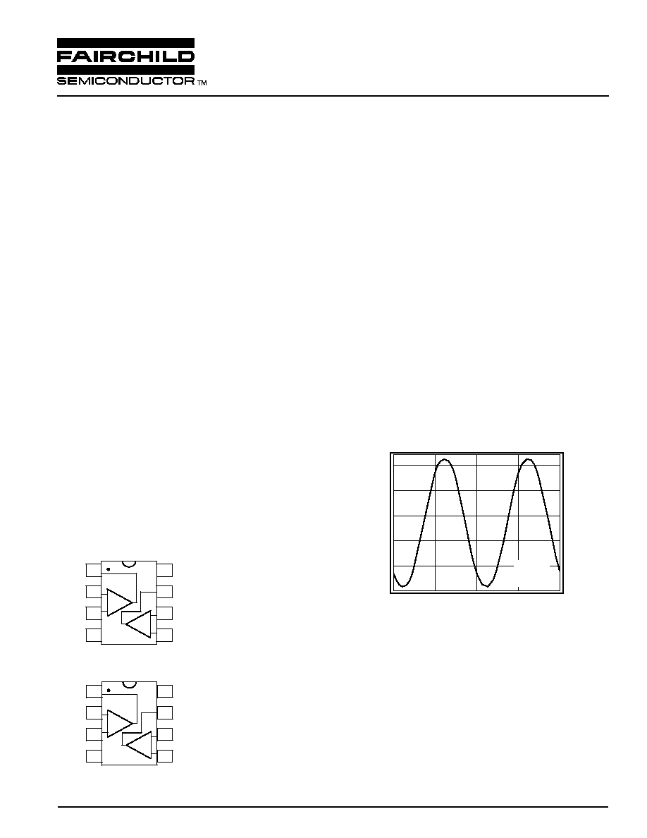
Output Swing
Output Voltage (0.5V/div)
Time (0.5
µ
s/div)
2.7
0
V
s
= +2.7V
R
L
= 2k
G = -1

DATA SHEET
KM4200
2
REV. 1A February 2001
PARAMETERS
CONDITIONS TYP
MIN
&
MAX
UNITS
NOTES
Case Temperature
+25°C
+25°C
Frequency Domain Response
-3dB bandwidth
G = +1, Vo = 0.05V
pp
215
MHz
1
G = +2, Vo = 0.2V
pp
85
MHz
full power bandwidth
G = +2, Vo = 2V
pp
36
MHz
gain bandwidth product
86
MHz
Time Domain Response
rise and fall time
0.2V step
3.7
ns
1
settling time to 0.1%
1V step
40
ns
overshoot
0.2V step,
9
%
slew rate
2.7V step
,
G = -1
130
V/
µ
s
Distortion and Noise Response
2nd harmonic distortion
1V
pp
, 5MHz
79
dBc
1
3rd harmonic distortion
1V
pp
, 5MHz
82
dBc
1
THD
1V
pp
, 5MHz
77
dB
1
input voltage noise
>1MHz
16
nV/
Hz
input current noise
>1MHz
1.3
pA/
Hz
crosstalk
10MHz
65
dB
1
DC Performance
input offset voltage
-1.6
±8
mV
2
average drift
10
µ
V/°C
input bias current
3
±8
µ
A
2
average drift
7
nA/°C
input offset current
0.1
±1
µ
A
2
power supply rejection ratio
DC
57
52
dB
2
open loop gain
75
65
dB
2
quiescent current per amplifier
3.9
5
mA
2
Input Characteristics
input resistance
4.3
M
input capacitance
1.8
pF
input common mode voltage range
-0.3 to 1.5
V
common mode rejection ratio
DC, V
cm
= 0V to V
s
- 1.5
87
72
dB
2
Output Characteristics
output voltage swing
R
L
= 10k
to V
s
/2
0.023 to 2.66
V
R
L
= 2k
to V
s
/2
0.025 to 2.653
0.1 to 2.6
V
2
R
L
= 150
to V
s
/2
0.065 to 2.55
0.3 to 2.325
V
2
linear output current
±55
mA
-40°C to +85°C
±50
mA
short circuit output current
±85
mA
power supply operating range
2.7
2.5 to 5.5
V
Min/max ratings are based on product characterization and simulation. Individual parameters are tested as noted. Outgoing quality levels
are determined from tested parameters.
NOTES:
1) Rf = 1k
was used used for optimal performance. (For G = +1, Rf = 0)
2) 100% tested at +25°C.
Absolute Maximum Ratings
Package Thermal Resistance
supply voltage
0 to +6V
Package
JA
maximum junction temperature
+175°C
8 lead SOIC
152°C/W
storage temperature range
-65°C to +150°C
8 lead MSOP
206°C/W
lead temperature (10 sec)
+300°C
operating temperature range (recommended) -40°C to +85°C
input voltage range
+V
s
+0.5V; -V
s
-0.5V
internal power dissipation
see power derating curves
KM4200 Electrical Characteristics
(V
s
= +2.7V, G = 2, R
L
= 2k
to V
s
/2; unless noted)

KM4200
DATA SHEET
REV. 1A February 2001
3
Parameters
Conditions
TYP
Min & Max
UNITS
NOTES
Case Temperature
+25°C
+25°C
Frequency Domain Response
-3dB bandwidth
G = +1, Vo = 0.05V
pp
260
MHz
1
G = +2, Vo = 0.2V
pp
90
MHz
full power bandwidth
G = +2, Vo = 2V
pp
40
MHz
gain bandwidth product
90
MHz
Time Domain Response
rise and fall time
0.2V step
3.6
ns
1
settling time to 0.1%
2V step
40
ns
overshoot
0.2V step,
7
%
slew rate
5V step
,
G = -1
145
V/
µ
s
Distortion and Noise Response
2nd harmonic distortion
2V
pp
, 5MHz
71
dBc
1
3rd harmonic distortion
2V
pp
, 5MHz
78
dBc
1
THD
2V
pp
, 5MHz
70
dB
1
input voltage noise
>1MHz
16
nV/
Hz
input current noise
>1MHz
1.3
pA/
Hz
crosstalk
10MHz
62
dB
1
DC Performance
input offset voltage
1.4
±8
mV
2
average drift
10
µ
V/°C
input bias current
3
±8
µ
A
2
average drift
7
nA/°C
input offset current
0.1
±0.8
µ
A
2
power supply rejection ratio
DC
57
52
dB
2
open loop gain
78
68
dB
2
quiescent current per amplifier
4.2
5.2
mA
2
Input Characteristics
input resistance
4.3
M
input capacitance
1.8
pF
input common mode voltage range
-0.3 to 3.8
V
common mode rejection ratio
DC, V
cm
= 0V to V
s
- 1.5
87
72
dB
2
Output Characteristics
output voltage swing
R
L
= 10k
to V
s
/2
0.027 to 4.97
V
R
L
= 2k
to V
s
/2
0.036 to 4.953
0.1 to 4.9
V
2
R
L
= 150
to V
s
/2
0.12 to 4.8
0.3 to 4.625
V
2
linear output current
±55
mA
-40°C to +85°C
±50
mA
short circuit output current
±85
mA
power supply operating range
5
2.5 to 5.5
V
Min/max ratings are based on product characterization and simulation. Individual parameters are tested as noted. Outgoing quality levels
are determined from tested parameters.
NOTES:
1) Rf = 1k
was used used for optimal performance. (For G = +1, Rf = 0)
2) 100% tested at +25°C.
KM4200 Electrical Characteristics
(V
s
= +5V, G = 2, R
L
= 2k
to V
s
/2; unless noted)
KM4200 Performance Characteristics
(V
s
= +5V, G = 2, R
f
= 2k
, R
L
= 2k
to V
s
/2; unless noted)
Non-Inverting Freq. Response V
s
= +5V
Normalized Magnitude (2dB/div)
Frequency (MHz)
0.1
1
G = 10
R
f
= 2k
10
100
G = 5
R
f
= 2k
G = 1
R
f
= 0
G = 2
R
f
= 1k
Inverting Frequency Response V
s
= +5V
Normalized Magnitude (1dB/div)
Frequency (MHz)
0.1
1
G = -10
R
f
= 2k
10
100
G = -5
R
f
= 2k
G = -2
R
f
= 2k
G = -1
R
f
= 2k
Non-Inverting Freq. Response V
s
= +2.7
Normalized Magnitude (2dB/div)
Frequency (MHz)
1
10
100
0.1
G = 10
R
f
= 2k
G = 5
R
f
= 2k
G = 1
R
f
= 0
G = 2
R
f
= 1k
Inverting Frequency Response V
s
= +2.7V
Normalized Magnitude (1dB/div)
Frequency (MHz)
0.1
1
G = -10
R
f
= 2k
10
100
G = -5
R
f
= 2k
G = -2
R
f
= 2k
G = -1
R
f
= 2k
Frequency Response vs. C
L
Magnitude (1dB/div)
Frequency (MHz)
0.1
1
10
100
C
L
= 100pF
R
s
= 25
C
L
= 50pF
R
s
= 33
C
L
= 20pF
R
s
= 20
C
L
= 10pF
R
s
= 0
+
-
1k
1k
R
s
C
L
R
L
Large Signal Frequency Response
Magnitude (1dB/div)
Frequency (MHz)
0.1
1
10
100
V
o
= 1V
pp
V
o
= 2V
pp
Frequency Response vs. Temperature
Magnitude (0.5dB/div)
Frequency (MHz)
1
10
100
Input Voltage Noise
Voltage Noise (nV/
Hz)
Frequency (Hz)
1k
10k
100k
1M
0
10
20
30
40
50
60
70
80
90
100
DATA SHEET
KM4200
4
REV. 1A February 2001
KM4200 Performance Characteristics
(V
s
= +5V, G = 2, R
f
= 2k
, R
L
= 2k
to V
s
/2; unless noted)
2nd & 3rd Harmonic Distortion; V
s
= +5V
Distortion (dBc)
Frequency (MHz)
0
5
10
15
3rd
R
L
= 150
20
2nd
R
L
= 150
3rd
R
L
= 2k
2nd
R
L
= 2k
-90
-80
-70
-60
-50
-40
-30
-20
V
o
= 2V
pp
R
f
= 1k
2nd & 3rd Harmonic Distortion; V
s
= +2.7V
Distortion (dBc)
Frequency (MHz)
0
5
10
15
2nd
R
L
= 150
20
3rd
R
L
= 150
3rd
R
L
= 2k
2nd
R
L
= 2k
-90
-80
-70
-60
-50
-40
-30
-20
V
o
= 1V
pp
R
f
= 1k
2nd Harmonic Distortion vs. V
o
Distortion (dBc)
Output Amplitude (V
pp
)
0.5
1.0
1.5
2.0
20MHz
10MHz
5MHz
2.5
-90
-80
-70
-60
-50
-40
-30
-20
R
f
= 1k
2MHz
3rd Harmonic Distortion vs. V
o
Distortion (dBc)
Output Amplitude (V
pp
)
0.5
1.0
1.5
2.0
20MHz
10MHz
5MHz
2.5
-90
-80
-70
-60
-50
-40
-30
-20
R
f
= 1k
2MHz
PSRR
PSRR (dB)
Frequency (MHz)
1k
0.01
0.1
1
100
-70
-60
-50
-40
-30
-20
-10
0
10
CMRR
CMRR (dB)
Frequency (MHz)
0.01
0.1
1.0
10
100
-90
-80
-70
-60
-50
-40
Open Loop Gain & Phase vs. Frequency
Open Loop Gain (dB)
Frequency (MHz)
-20
-10
0
10
20
-180
-135
-90
-45
0
30
40
50
60
70
80
0.01
0.1
1
10
100
Phase (degrees)
|Gain|
Phase
Output Current
Output Voltage (V)
Output Current (mA)
-100
-50
0
50
100
Linear output current 55mA
-0.8
-0.6
-0.2
0
0.2
0.4
0.6
0.8
-0.4
Short circuit current 85mA
KM4200
DATA SHEET
REV. 1A February 2001
5