 | ÐлекÑÑоннÑй компоненÑ: KM4211IM8 | СкаÑаÑÑ:  PDF PDF  ZIP ZIP |
Äîêóìåíòàöèÿ è îïèñàíèÿ www.docs.chipfind.ru
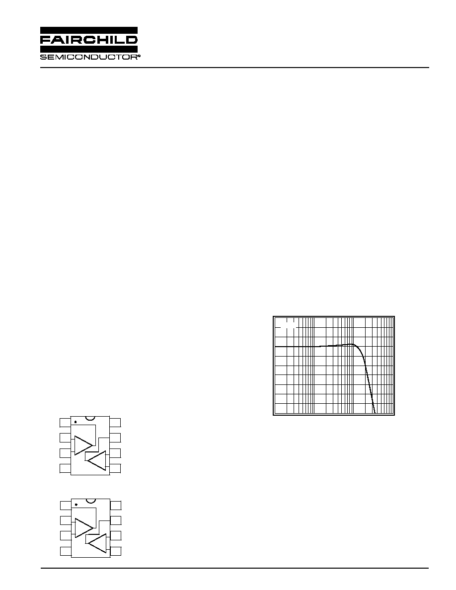
Non-Inverting Freq. Response V
s
= +5V
Normalized Magnitude (2dB/div)
Frequency (MHz)
0.1
1
10
100
G = 2
Features
I
208
µA supply current
I
35MHz bandwidth
I
Fully specified at +2.7V and +5V supplies
I
Output voltage range: 0.08V to 4.88V; V
s
= +5
I
Input voltage range: -0.3V to +3.8V; V
s
= +5
I
27V/
µs slew rate
I
±8.5mA linear output current
I
±13mA short circuit output current
I
21nV/
Hz input voltage noise
I
Directly replaces OPA2350, MAX4132, MAX4281
I
Small package options (SOIC-8 and MSOP-8)
Applications
I
A/D buffer
I
Smart card readers
I
Active filters
I
Keyless entry
I
Signal conditioning
I
ASCI input devices
I
Portable test instruments
I
PCMUA cards
I
Portable communications
I
Bar-code readers
I
Portable/battery-powered applications
General Description
The KM4211 is a dual ultra-low power, low cost,
voltage feedback amplifier. The KM4211 uses only
208
µA of supply current per amplifier and is designed
to operate from 2.5V to 5.5V or ±1.25V to ±2.75V
supplies. The input voltage range extends 300mV below
the negative rail and 1.2V below the positive rail.
The KM4211 offers high bipolar performance at a
low CMOS price. The KM4211 offers superior
dynamic performance with a 35MHz small signal
bandwidth and 27V/
µs slew rate. The combination
of low power, high bandwidth, and rail-to-rail
performance make the KM4211 well suited for
battery-powered communication/computing systems.
The KM4112 (single) and KM4121 (single with disable)
are also available.
KM4211
Dual, 0.2mA, Low Cost, +2.7V & +5V, 35MHz Rail-to-Rail Amp
www.fairchildsemi.com
REV. 1 June 2001
KM4211 Packages
-
+
-
+
1
2
3
4
Out1
-In1
+In1
-V
s
+V
s
Out2
-In2
+In2
8
7
6
5
SOIC-8
-
+
-
+
1
2
3
4
Out1
-In1
+In1
-V
s
+V
s
Out2
-In2
+In2
8
7
6
5
MSOP-8

DATA SHEET
KM4211
2
REV. 1 June 2001
PARAMETERS
CONDITIONS
TYP
MIN & MAX
UNITS
NOTES
Case Temperature
+25°C
+25°C
Frequency Domain Response
-3dB bandwidth
G = +1, Vo = 0.05V
pp
28
MHz
1
G = +2, Vo < 0.2V
pp
15
MHz
full power bandwidth
G = -1, Vo = 2V
pp
7 MHz
gain bandwidth product
16
MHz
Time Domain Response
rise and fall time
0.2V step
20
ns
settling time to 0.1%
1V step
140
ns
overshoot
2V step, G = -1
<1
%
slew rate
2V step, G = -1
20
V/
µs
Distortion and Noise Response
2nd harmonic distortion
1V
pp
, 100kHz
85
dBc
3rd harmonic distortion
1V
pp
, 100kHz
63
dBc
THD
1V
pp
, 100kHz
62
dB
input voltage noise
>10kHz
23
nV/
Hz
crosstalk
100kHz, Vo = 0.2V
pp
98
dB
DC Performance
input offset voltage
0.8
±5
mV
2
average drift
11
µV/°C
input bias current
0.4
1.3
µA
2
average drift
1
nA/°C
input offset current
8
130
nA
2
power supply rejection ratio
DC
60
56
dB
2
open loop gain
65
56
dB
2
quiescent current
185
245
µA
2
Input Characteristics
input resistance
>10
M
input capacitance
1.5
pF
input common mode voltage range
-0.3 to 1.5
V
common mode rejection ratio
DC, V
cm
= 0V to V
s
- 1.5
92
65
dB
2
Output Characteristics
output voltage swing
R
L
= 10k
to V
s
/2
0.06 to 2.62
V
R
L
= 2k
to V
s
/2
0.08 to 2.6
0.2 to 2.4
V
2
linear output current
±8
mA
short circuit output current
±12.5
mA
power supply operating range
2.7
2.5 to 5.5
V
Min/max ratings are based on product characterization and simulation. Individual parameters are tested as noted. Outgoing quality levels
are determined from tested parameters.
NOTES:
1) For G = +1, Rf = 0.
2) 100% tested at +25°C.
Absolute Maximum Ratings
Package Thermal Resistance
supply voltage
0 to +6V
Package
JA
maximum junction temperature
+175°C
8 lead SOIC
152°C/W
storage temperature range
-65°C to +150°C
8 lead MSOP
206°C/W
lead temperature (10 sec)
+260°C
operating temperature range (recommended) -40°C to +85°C
input voltage range
+V
s
+0.5V; -V
s
-0.5V
internal power dissipation
see power derating curves
KM4211 Electrical Characteristics
(V
s
= +2.7V, G = 2, R
L
= 2k
to V
s
/2, R
f
= 2.5k
; unless noted)

KM4211
DATA SHEET
REV. 1 June 2001
3
PARAMETERS
CONDITIONS
TYP
MIN & MAX
UNITS
NOTES
Case Temperature
+25°C
+25°C
Frequency Domain Response
-3dB bandwidth
G = +1, Vo = 0.05V
pp
35
MHz
1
G = +2, Vo < 0.2V
pp
18
MHz
full power bandwidth
G = -1, Vo = 2V
pp
8 MHz
gain bandwidth product
20
MHz
Time Domain Response
rise and fall time
0.2V step
18
ns
settling time to 0.1%
2V step
140
ns
overshoot
2V step, G = -1
<1
%
slew rate
2V step, G = -1
27
V/
µs
Distortion and Noise Response
2nd harmonic distortion
2V
pp
, 100kHz
78
dBc
3rd harmonic distortion
2V
pp
, 100kHz
66
dBc
THD
2V
pp
, 100kHz
65
dB
input voltage noise
>10kHz
21
nV/
Hz
crosstalk
100kHz, Vo = 0.2V
pp
98
dB
DC Performance
input offset voltage
-1.5
mV
average drift
20
µV/°C
input bias current
0.4
µA
average drift
1
nA/°C
input offset current
7
nA
power supply rejection ratio
DC
60
dB
open loop gain
62
dB
quiescent current
208
µA
Input Characteristics
input resistance
>10
M
input capacitance
1.35
pF
input common mode voltage range
-0.3 to 3.8
V
common mode rejection ratio
DC, V
cm
= 0V to V
s
- 1.5
85
dB
Output Characteristics
output voltage swing
R
L
= 10k
to V
s
/2
0.08 to 4.88
V
R
L
= 2k
to V
s
/2
0.1 to 4.8
V
linear output current
±8.5
mA
short circuit output current
±13
mA
power supply operating range
5
2.5 to 5.5
V
Min/max ratings are based on product characterization and simulation. Individual parameters are tested as noted. Outgoing quality levels
are determined from tested parameters.
NOTES:
1) For G = +1, Rf = 0.
KM4211 Electrical Characteristics
(V
s
= +2.7V, G = 2, R
L
= 2k
to V
s
/2, R
f
= 2.5k
; unless noted)
4
REV. 1 June 2001
KM4211 Performance Characteristics
(V
s
= +5V, G = 2, R
L
= 2k
to V
s
/2, R
f
= 2.5k
; unless noted)
Non-Inverting Frequency Response V
s
= +5V
Normalized Magnitude (2dB/div)
Frequency (MHz)
0.1
1
G = 10
10
100
G = 5
G = 1
R
f
= 0
G = 2
Inverting Frequency Response V
s
= +5V
Normalized Magnitude (1dB/div)
Frequency (MHz)
0.1
1
G = -10
10
100
G = -5
G = -2
G = -1
Non-Inverting Freq. Response V
s
= +2.7V
Normalized Magnitude (2dB/div)
Frequency (MHz)
0.1
1
G = 10
10
100
G = 5
G = 2
G = 1
R
f
= 0
Inverting Frequency Response V
s
= +2.7V
Normalized Magnitude (1dB/div)
Frequency (MHz)
0.1
1
G = -10
10
100
G = -5
G = -1
G = -2
Large Signal Frequency Response
Magnitude (1dB/div)
Frequency (MHz)
0.1
1
10
100
V
o
= 1V
pp
V
o
= 2V
pp
Open Loop Gain & Phase vs. Frequency
Open Loop Gain (dB)
Frequency (Hz)
10
100
1k
1M
100k
10k
10M
-20
0
20
100
40
80
60
Open Loop
Ph
a
s
e (de
g
)
-200
-160
-120
40
-80
0
-40
|Gain|
Phase
Input Voltage Noise
Voltage Noise (nV/
Hz)
Frequency (Hz)
100
1k
10k
1M
0
20
40
60
80
100
100k
2nd & 3rd Harmonic Distortion; V
s
= +5V
Distortion (dBc)
Frequency (kHz)
10
100
3rd
1000
2nd
-100
-90
-80
-70
-60
-50
-40
V
o
= 2V
pp
DATA SHEET
KM4211
KM4211
DATA SHEET
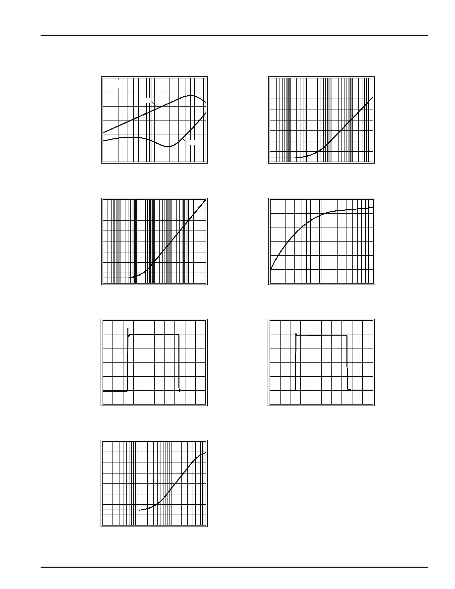
KM4211 Performance Characteristics
(V
s
= +5V, G = 2, R
L
= 2k
to V
s
/2, R
f
= 2.5k
; unless noted)
2nd & 3rd Harmonic Distortion; V
s
= +2.7V
Distortion (dBc)
Frequency (kHz)
10
100
3rd
1000
2nd
-100
-90
-80
-70
-60
-50
-40
V
o
= 1V
pp
PSRR
PSRR (dB)
Frequency (Hz)
100
1k
10k
1M
100k
10M
-70
-60
-50
-40
-30
10
-20
-10
0
CMRR
CMRR (dB)
Frequency (Hz)
10
100
1k
1M
100k
10k
10M
-100
-90
-80
-70
-20
-60
-50
-30
-40
Output Swing vs. R
L
Output Swing (V
pp
)
R
L
(k
)
1
10
100
4.55
4.60
4.70
4.85
4.75
4.80
4.65
Small Signal Pulse Response V
s
= +5V
Output Voltage (0.05V/div)
Time (1
µs/div)
Large Signal Pulse Response V
s
= +5V
Output Voltage (0.5V/div)
Time (1
µs/div)
Crosstalk vs. Frequency
Crosstalk (dB)
Frequency (MHz)
0.01
0.1
1
10
-105
-100
-95
-90
-65
-85
-80
-70
-75
KM4211
DATA SHEET
REV. 1 June 2001
5