 | ÐлекÑÑоннÑй компоненÑ: KM4270 | СкаÑаÑÑ:  PDF PDF  ZIP ZIP |
Äîêóìåíòàöèÿ è îïèñàíèÿ www.docs.chipfind.ru
Features at 2.7V
· 136
µ
A supply current per amplifier
· 4.9MHz bandwidth
· Output swings to within 20mV of either rail
· Input voltage range exceeds the rail by >250mV
· 5.3V/
µ
s slew rate
· 16mA output current
· 21nV/
Hz input voltage noise
· KM4170:
directly replaces OPA340, OPA343, and TLV2461 in
single supply applications and available in SC70-5 and
SOT23-5 package options
· KM4270:
directly replaces MAX4126, OPA2340, LMV822 and
TLV2462 in single supply applications and available in
SOIC-8 and MSOP-8 package options
· KM4470:
directly replaces MAX4129, OPA4340, LMV824 and
TLV2464 in single supply applications and available in
TSSOP-14 package option
Applications
· Portable/battery-powered applications
· PCMCIA, USB
· Mobile communications, cellular phones, pagers
· Notebooks and PDA's
· Sensor Interface
· A/D buffer
· Active filters
· Signal conditioning
· Portable test instruments
Description
The KM4170 (single), KM4270 (dual), and KM4470 (quad)
are ultra-low cost, low power, voltage feedback amplifiers.
At 5V, the KM4X70 family uses only 160
µ
A of supply current
per amplifier and are designed to operate from a supply range
of 2.5V to 5.5V (±1.25 to ±2.75). The input voltage range
exceeds the negative and positive rails.
The KM4X70 family of amplifiers offer high bipolar
performance at a low CMOS prices. They offer superior
dynamic performance with 4.9MHz small signal bandwidths
and 5.3V/
µ
s slew rates. The combination of low power, high
bandwidth, and rail-to-rail performance make the KM4X70
amplifiers well suited for battery-powered communication/
computing systems.
KM4170, KM4270, KM4470
Low Cost, +2.7V & +5V, Rail-to-Rail I/O Amplifiers
www.fairchildsemi.com
REV. 5 December 2002
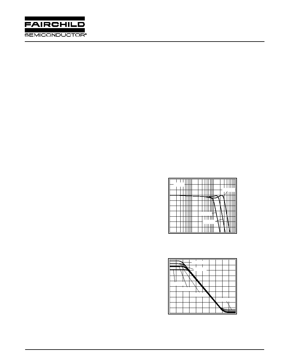
Large Signal Frequency Response
Magnitude (1dB/div)
Frequency (MHz)
0.01
0.1
1
10
V
o
= 4V
pp
V
s
= 5V
V
o
= 1V
pp
V
o
= 2V
pp
Output Swing vs. Load
Output Voltage (0.27V/div)
Input Voltage (0.4V/div)
-2.0
0
2.0
-1.35
0
1.35
R
L
= 10k
R
L
= 1k
R
L
= 75/100
R
L
= 200
R
L
= 100
R
L
= 75
DATA SHEET
KM4170, KM4270, KM4470
2
REV. 5 December 2002
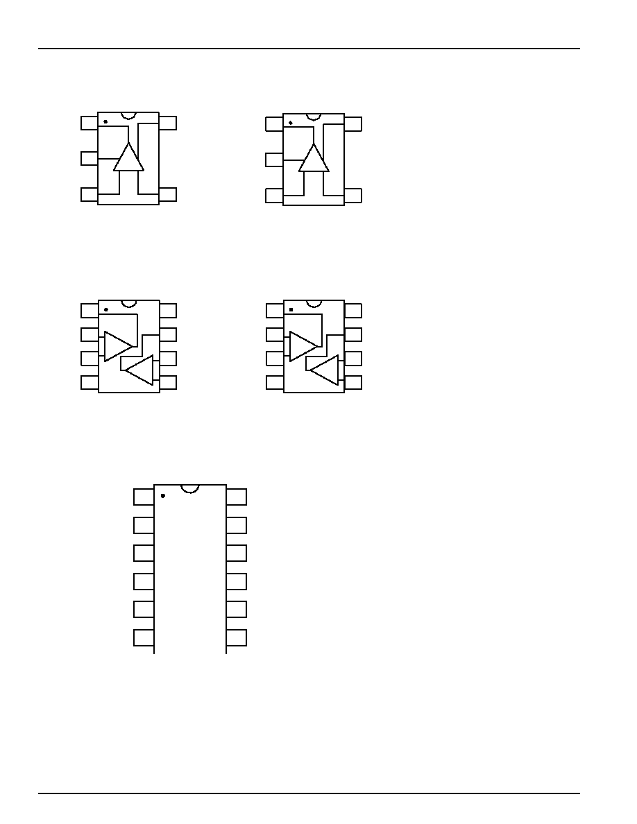
KM4170
-
+
1
2
3
Out
-V
s
+In
+V
s
-In
5
4
-
+
1
2
3
Out
-V
s
+In
+V
s
-In
5
4
SC70-5
KM4270
-
+
-
+
1
2
3
4
Out1
-In1
+In1
-V
s
+V
s
Out2
-In2
+In2
8
7
6
5
MSOP
-
+
-
+
1
2
3
4
Out1
-In1
+In1
-V
s
+V
s
Out2
-In2
+In2
8
7
6
5
SOIC
KM4470
1
2
3
4
Out1
-In1
+In1
+V
s
14
13
12
11
5
6
+In2
-In2
10
9
TSSOP
SOT23-5
KM4170, KM4270, KM4470
DATA SHEET
REV. 5 December 2002
3
Absolute Maximum Ratings
Parameter
Min.
Max.
Unit
Supply Voltages
0
+6
V
Maximum Junction Temperature
+175
°C
Storage Temperature Range
-65
+150
°C
Lead Temperature, 10 seconds
+260
°C
Operating Temperature Range, recommended
-40
+85
°C
Input Voltage Range
-Vs -0.5 +Vs +0.5
V
Iout Continuous
-30
+30
mA
Electrical Specifications
(V
s
= +2.7V, G = 2, R
L
= 10k
to V
s
/2, R
f
= 5k
; unless otherwise noted)
Parameter
Conditions
Min.
Typ.
Max.
Unit
AC Performance
-3dB Bandwidth
1
G = +1, V
o
= 0.02V
pp
4.9
MHz
G = +2, V
o
= 0.2V
pp
3.7
MHz
Full Power Bandwidth
G = +2, V
o
= 2V
pp
1.4 MHz
Gain Bandwidth Product
2.2
MHz
Rise and Fall Time
1V step
163
ns
Overshoot
1V step
<1
%
Slew Rate
1V step
5.3
V/
µ
s
2nd Harmonic Distortion
1V
pp
, 10kHz
-72
dBc
3rd Harmonic Distortion
1V
pp
, 10kHz
-72
dBc
THD
1V
pp
, 10kHz
0.03
%
Input Voltage Noise
>10kHz
21
nV/
Hz
DC Performance
Input Offset Voltage
2
-6
0.5
+6
mV
Average Drift
5
µ
V/°C
Input Bias Current
2
90
420
nA
Average Drift
32
pA/°C
Power Supply Rejection Ratio
2
DC
55
83
dB
Open Loop Gain
R
L
= 10k
90
dB
Quiescent Current Per Channel
2
136
190
µ
A
Input Characteristics
Input Resistance
12
M
Input Capacitance
2
pF
Input Common Mode Voltage Range
-0.25 to 2.95
V
Common Mode Rejection Ratio
2
DC, V
cm
= 0V to V
s
55
81
dB
Output Characteristics
Output Voltage Swing
2
R
L
= 10k
to V
s
/2
0.06 to 2.64 0.02 to 2.68
V
R
L
= 1k
to V
s
/2
0.05 to 2.63
V
R
L
= 200
to V
s
/2
0.11 to 2.52
V
Output Current
±16
mA
Power Supply Operating Range
2.5
2.7
5.5
V
Min/max ratings are based on product characterization and simulation. Individual parameters are tested as noted. Outgoing quality levels are
determined from tested parameters.
Notes:
1. For G = +1, Rf = 0.
2. For RL = 10k
, KM4170, KM4270, and KM4470 are 100% tested at 25°C.

DATA SHEET
KM4170, KM4270, KM4470
4
REV. 5 December 2002
Electrical Specifications
(V
s
= +5V, G = 2, R
L
= 10k
to V
s
/2, R
f
= 5k
; unless otherwise noted)
Parameter
Conditions
Min.
Typ.
Max.
Unit
AC Performance
-3dB Bandwidth
1
G = +1, V
o
= 0.02V
pp
4.3
MHz
G = +2, V
o
= 0.2V
pp
3.0
MHz
Full Power Bandwidth
G = +2, V
o
= 2V
pp
2.3 MHz
Gain Bandwidth Product
2.0
MHz
Rise and Fall Time
1V step
110
ns
Overshoot
1V step
<1
%
Slew Rate
1V step
9
V/
µ
s
2nd Harmonic Distortion
1V
pp
, 10kHz
-73
dBc
3rd Harmonic Distortion
1V
pp
, 10kHz
-75
dBc
THD
1V
pp
, 10kHz
0.03
%
Input Voltage Noise
>10kHz
22
nV/
Hz
DC Performance
Input Offset Voltage
2
-8
1.5
+8
mV
Average Drift
15
µ
V/°C
Input Bias Current
2
90
450
nA
Average Drift
40
pA/°C
Power Supply Rejection Ratio
2
DC
40
60
dB
Open Loop Gain
R
L
= 10k
80
dB
Quiescent Current Per Channel
2
160
235
µ
A
Input Characteristics
Input Resistance
12
M
Input Capacitance
2
pF
Input Common Mode Voltage Range
-0.25 to 5.25
V
Common Mode Rejection Ratio
2
DC, V
cm
= 0V to V
s
58
85
dB
Output Characteristics
Output Voltage Swing
2
R
L
= 10k
to V
s
/2
0.08 to 4.92 0.04 to 4.96
V
R
L
= 1k
to V
s
/2
0.07 to 4.9
V
R
L
= 200
to V
s
/2
0.14 to 4.67
V
Output Current
±30
mA
Power Supply Operating Range
2.5
2.7
5.5
V
Min/max ratings are based on product characterization and simulation. Individual parameters are tested as noted. Outgoing quality levels are
determined from tested parameters.
Notes:
1. For G = +1, Rf = 0.
2. For RL = 10k
, KM4170 is 100% tested at 25°C.
Package Thermal Resistance
Package
JA
5 lead SOT23
256°C/W
5 lead SC70
331.4°C/W
8 lead SOIC
152°C/W
8 lead MSOP
206°C/W
14 lead TSSOP
100°C/W
KM4170, KM4270, KM4470
DATA SHEET
REV. 5 December 2002
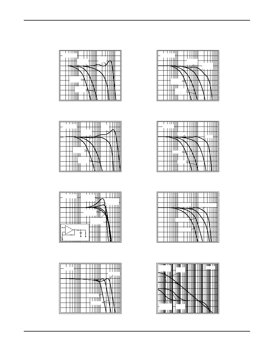
5
Non-Inverting Freq. Response V
s
= +5V
Normalized Magnitude (1dB/div)
Frequency (MHz)
0.01
0.1
G = 10
R
f
= 5k
1
10
G = 5
R
f
= 5k
G = 1
R
f
= 0
G = 2
R
f
= 5k
V
o
= 0.2V
pp
Inverting Frequency Response V
s
= +5V
Normalized Magnitude (1dB/div)
Frequency (MHz)
0.01
0.1
G = -10
R
f
= 5k
1
10
G = -5
R
f
= 5k
G = -1
R
f
= 5k
G = -2
R
f
= 5k
V
o
= 0.2V
pp
Non-Inverting Frequency Response
Normalized Magnitude (1dB/div)
Frequency (MHz)
0.01
0.1
G = 10
R
f
= 5k
1
10
G = 5
R
f
= 5k
G = 1
R
f
= 0
G = 2
R
f
= 5k
V
o
= 0.2V
pp
Inverting Frequency Response
Normalized Magnitude (1dB/div)
Frequency (MHz)
0.01
0.1
G = -10
1
10
G = -5
G = -1
G = -2
R
f
= 5k
Frequency Response vs. C
L
Magnitude (1dB/div)
Frequency (MHz)
0.01
0.1
1
10
C
L
= 100pF
R
s
= 100
C
L
= 10pF
R
s
= 0
C
L
= 50pF
R
s
= 0
C
L
= 20pF
R
s
= 0
+
-
5k
5k
R
s
C
L
R
L
V
o
= 0.05V
Frequency Response vs. R
L
Magnitude (1dB/div)
Frequency (MHz)
0.01
0.1
1
10
R
L
= 1k
R
L
= 50
R
L
= 10k
R
L
= 200
Large Signal Frequency Response
Magnitude (1dB/div)
Frequency (MHz)
0.01
0.1
1
10
V
o
= 4V
pp
V
s
= 5V
V
o
= 1V
pp
V
o
= 2V
pp
Open Loop Gain & Phase vs. Frequency
Open Loop Gain (dB)
Frequency (Hz)
10
0
10
1
10
2
10
3
10
4
10
5
10
6
10
7
10
8
-20
60
140
Phase
No load
0
Open Loop Phase (deg)
-180
-90
0
-135
-45
|Gain|
No load
Phase
R
L
= 10k
|Gain|
R
L
= 10k
V
s
= 5V
20
40
80
120
100
Typical Operating Characteristics
(V
s
= +2.7V, G = 2, R
L
= 10k
to V
s
/2, R
f
= 5k
; unless otherwise noted)