Äîêóìåíòàöèÿ è îïèñàíèÿ www.docs.chipfind.ru
Features
I
136
µA supply current
I
4.9MHz bandwidth
I
Output swings to within 20mV of either rail
I
Input voltage range exceeds the rail by >250mV
I
5.3V/
µs slew rate
I
35mA short circuit output current
I
24nV/
Hz input voltage noise
I
Directly replaces LMC7101 in single supply
applications
I
Available in SOT23-5 package
Applications
I
Portable/battery-powered applications
I
PCMCIA, USB
I
Mobile communications, cellular phones, pagers
I
Notebooks and PDA's
I
Sensor Interface
I
A/D buffer
I
Active filters
I
Signal conditioning
I
Portable test instruments
General Description
The KM7101 is an ultra-low cost, low power, voltage
feedback amplifier that is pin compatible to the
LMC7101. If a standard pinout is required, use the
KM4170. The KM7101 uses only 136
µA of supply
current and offers no crossover distortion. The input
common mode voltage range exceeds the negative
and positive rails.
The KM7101 offers high bipolar performance at a
low CMOS price. The KM7101 offers superior
dynamic performance with a 4.9MHz small signal
bandwidth and 5.3V/
µs slew rate. The combination
of low power, high bandwidth, and rail-to-rail per-
formance make the KM7101 well suited for battery-
powered communication/computing systems.
KM7101
Ultra-Low Cost, 139
µA, +2.7V, 4.9MHz Rail-to-Rail I/O Amplifier
www.fairchildsemi.com
REV. 1B March 2001
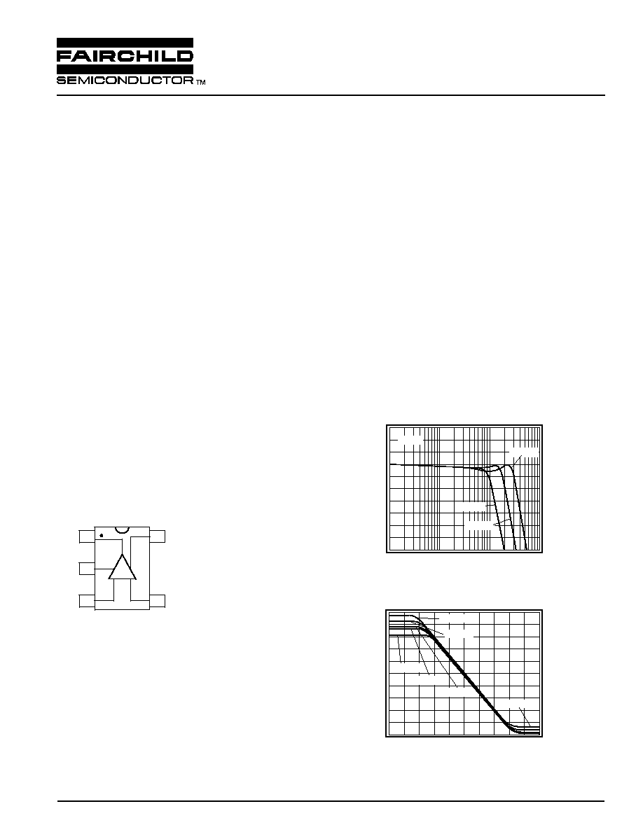
KM7101 Package
-
+
1
2
3
Out
+V
s
+In
-V
s
-In
5
4
SOT23-5
Large Signal Frequency Response
Magnitude (1dB/div)
Frequency (MHz)
0.01
0.1
1
10
V
o
= 4V
pp
V
s
= 5V
V
o
= 1V
pp
V
o
= 2V
pp
Output Swing vs. Load
Output Voltage (0.27V/div)
Input Voltage (0.4V/div)
-2.0
0
2.0
-1.35
0
1.35
R
L
= 10k
R
L
= 1k
R
L
= 75/100
R
L
= 200
R
L
= 100
R
L
= 75

DATA SHEET
KM7101
2
REV. 1B March 2001
Parameters
Conditions
TYP
Min & Max
UNITS
NOTES
Case Temperature
+25°C
+25°C
Frequency Domain Response
-3dB bandwidth
G = +1, Vo = 0.02V
pp
4.9
MHz
1
G = +2, Vo = 0.2V
pp
3.7
MHz
full power bandwidth
G = +2, Vo = 2V
pp
1.4 MHz
gain bandwidth product
2.2
MHz
Time Domain Response
rise and fall time
1V step
163
ns
overshoot
1V step
<1
%
slew rate
1V step
5.3 V/
µs
Distortion and Noise Response
2nd harmonic distortion
1V
pp
, 10kHz
-75
dBc
3rd harmonic distortion
1V
pp
, 10kHz
-76
dBc
THD
1V
pp
, 10kHz
0.03
%
input voltage noise
>1MHz
24
nV/
Hz
DC Performance
input offset voltage
0.5
±6
mV
2
average drift
5
µV/°C
input bias current
90
220
nA
2
average drift
32
pA/°C
power supply rejection ratio
DC
83
55
dB
2
open loop gain
R
L
= 10k
90
dB
quiescent current
136
190
µA
2
Input Characteristics
input resistance
12
M
input capacitance
2
pF
input common mode voltage range
-0.25 to 2.95
V
common mode rejection ratio
DC, V
cm
= 0V to V
s
81
55
dB
2
Output Characteristics
output voltage swing
R
L
= 10k
to V
s
/2
0.02 to 2.68
0.06 to 2.64
V
2
R
L
= 1k
to V
s
/2
0.05 to 2.63
V
R
L
= 200
to V
s
/2
0.11 to 2.52
V
output current
±16
mA
short circuit output current
±35
mA
power supply operating range
2.7
2.5 to 5.5
V
Min/max ratings are based on product characterization and simulation. Individual parameters are tested as noted. Outgoing quality levels
are determined from tested parameters.
NOTES:
1) For G = +1, Rf = 0.
2) 100% tested at +25°C.
Absolute Maximum Ratings
Package Thermal Resistance
supply voltage
0 to +6V
Package
JA
maximum junction temperature
+175°C
5 lead SOT23
256°C/W
storage temperature range
-65°C to +150°C
lead temperature (10 sec)
+300°C
operating temperature range (recommended) -40°C to +85°C
input voltage range
+V
s
+ 0.5V, -V
s
- 0.5V
internal power dissipation
see power derating curves
KM7101 Electrical Characteristics
(V
s
= +2.7V, G = 2, R
L
= 10k
to V
s
/2, R
f
= 5k
; unless noted)

KM7101
DATA SHEET
REV. 1B March 2001
3
Parameters
Conditions
TYP
Min & Max
UNITS
NOTES
Case Temperature
+25°C
+25°C
Frequency Domain Response
-3dB bandwidth
G = +1, Vo = 0.02V
pp
4.3
MHz
1
G = +2, Vo = 0.2V
pp
3.0
MHz
full power bandwidth
G = +2, Vo = 2V
pp
2.3
MHz
gain bandwidth product
2.0
MHz
Time Domain Response
rise and fall time
1V step
110
ns
overshoot
1V step
<1
%
slew rate
1V step
9
V/
µs
Distortion and Noise Response
2nd harmonic distortion
2V
pp
, 10kHz
-73
dBc
3rd harmonic distortion
2V
pp
, 10kHz
-75
dBc
THD
2V
pp
, 10kHz
0.03
%
input voltage noise
>1MHz
27
nV/
Hz
DC Performance
input offset voltage
1.5
±8
mV
2
average drift
15
µV/°C
input bias current
90
270
nA
2
average drift
40
pA/°C
power supply rejection ratio
DC
60
40
dB
2
open loop gain
R
L
= 10k
80
dB
quiescent current
160
235
µA
2
Input Characteristics
input resistance
12
M
input capacitance
2
pF
input common mode voltage range
-0.25 to 5.25
V
common mode rejection ratio
DC, V
cm
= 0V to V
s
85
58
dB
2
Output Characteristics
output voltage swing
R
L
= 10k
to V
s
/2
0.04 to 4.96 0.08 to 4.92
V
2
R
L
= 1k
to V
s
/2
0.07 to 4.9
V
R
L
= 200
to V
s
/2
0.14 to 4.67
V
output current
±30
mA
short circuit output current
±60
mA
power supply operating range
5.0
2.5 to 5.5
V
Min/max ratings are based on product characterization and simulation. Individual parameters are tested as noted. Outgoing quality levels
are determined from tested parameters.
NOTES:
1) For G = +1, Rf = 0.
2) 100% tested at +25°C.
KM7101 Electrical Characteristics
(V
s
= +5V, G = 2, R
L
= 10k
to V
s
/2, R
f
= 5k
; unless noted)
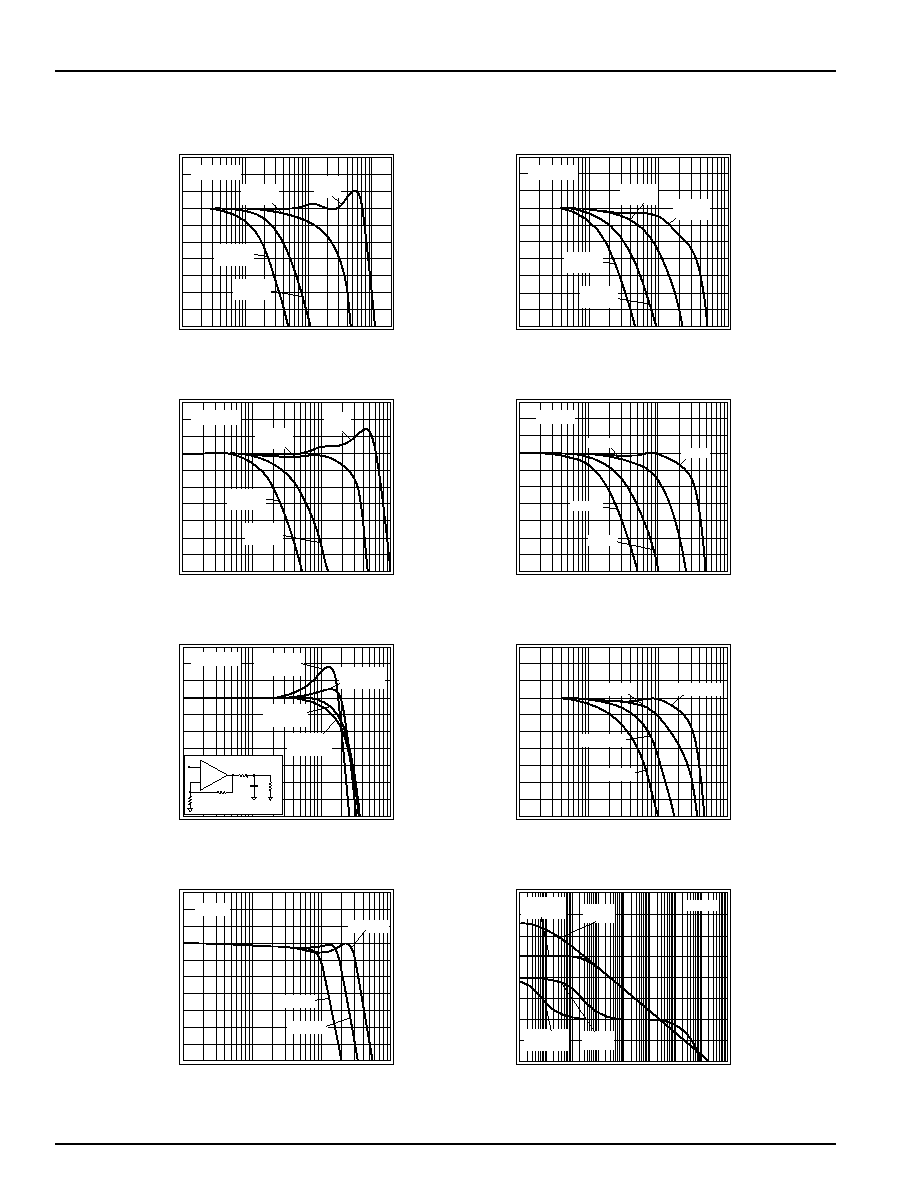
KM7101 Performance Characteristics
(V
s
= +2.7, G = 2, R
L
= 10k
to V
s
/2, R
f
= 5k
; unless noted)
Non-Inverting Freq. Response V
s
= +5V
Normalized Magnitude (1dB/div)
Frequency (MHz)
0.01
0.1
G = 10
R
f
= 5k
1
10
G = 5
R
f
= 5k
G = 1
R
f
= 0
G = 2
R
f
= 5k
V
o
= 0.2V
pp
Inverting Frequency Response V
s
= +5V
Normalized Magnitude (1dB/div)
Frequency (MHz)
0.01
0.1
G = -10
R
f
= 5k
1
10
G = -5
R
f
= 5k
G = -1
R
f
= 5k
G = -2
R
f
= 5k
V
o
= 0.2V
pp
Non-Inverting Freq. Response V
s
= +2.7V
Normalized Magnitude (1dB/div)
Frequency (MHz)
0.01
0.1
G = 10
R
f
= 5k
1
10
G = 5
R
f
= 5k
G = 1
R
f
= 0
G = 2
R
f
= 5k
V
o
= 0.2V
pp
Inverting Frequency Response V
s
= +2.7V
Normalized Magnitude (1dB/div)
Frequency (MHz)
0.01
0.1
G = -10
1
10
G = -5
G = -1
G = -2
R
f
= 5k
Frequency Response vs. C
L
Magnitude (1dB/div)
Frequency (MHz)
0.01
0.1
1
10
C
L
= 100pF
R
s
= 100
C
L
= 10pF
R
s
= 0
C
L
= 50pF
R
s
= 0
C
L
= 20pF
R
s
= 0
+
-
5k
5k
R
s
C
L
R
L
V
o
= 0.05V
Frequency Response vs. R
L
Magnitude (1dB/div)
Frequency (MHz)
0.01
0.1
1
10
R
L
= 1k
R
L
= 50
R
L
= 10k
R
L
= 200
Large Signal Frequency Response
Magnitude (1dB/div)
Frequency (MHz)
0.01
0.1
1
10
V
o
= 4V
pp
V
s
= 5V
V
o
= 1V
pp
V
o
= 2V
pp
Open Loop Gain & Phase vs. Frequency
Open Loop Gain (dB)
Frequency (Hz)
10
0
10
1
10
2
10
3
10
4
10
5
10
6
10
7
10
8
-20
60
140
Phase
No load
0
Open Loop Phase (deg)
-180
-90
0
-135
-45
|Gain|
No load
Phase
R
L
= 10k
|Gain|
R
L
= 10k
V
s
= 5V
20
40
80
120
100
DATA SHEET
KM7101
4
REV. 1B March 2001
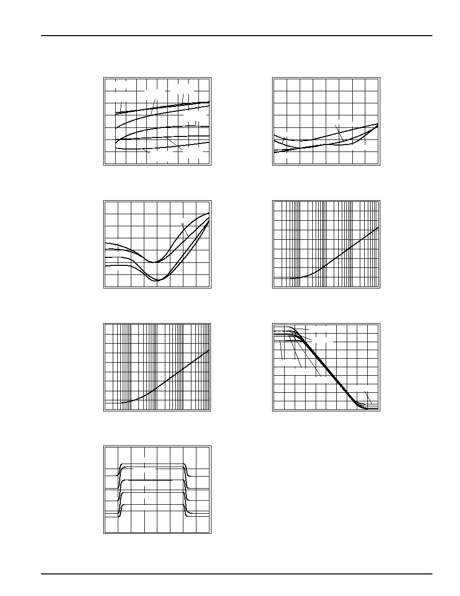
KM7101 Performance Characteristics
(V
s
= +2.7V, G = 2, R
L
= 10k
to V
s
/2, R
f
= 5k
; unless noted)
2nd & 3rd Harmonic Distortion; V
s
= +2.7V
Distortion (dBc)
Frequency (kHz)
0
20
40
60
80
3rd
R
L
= 1k
100
3rd
R
L
= 200
2nd
R
L
= 10k
2nd
R
L
= 1k
-90
-80
-70
-60
-50
-40
-30
-20
V
o
= 1V
pp
3rd
R
L
= 10k
2nd
R
L
= 200
2nd Harmonic Distortion vs. V
o
Distortion (dB)
Output Amplitude (V
pp
)
0.5
1
1.5
2
100kHz
50kHz
10kHz
2.5
-90
-80
-70
-60
-50
-40
-30
-20
10kHz, 20kHz
50kHz
3rd Harmonic Distortion vs. V
o
Distortion (dB)
Output Amplitude (V
pp
)
0.5
1
1.5
2
100kHz
50kHz
10kHz
2.5
-90
-80
-70
-60
-50
-40
-30
-20
20kHz
CMRR
CMRR (dB)
Frequency (Hz)
10
100
10000
1000
100000
-90
-80
-70
-60
0
-50
-40
-10
-30
-20
PSRR
PSRR (dB)
Frequency (Hz)
10
10000
1000
100
100000
-90
-70
-60
-50
-40
0
-30
-20
-10
-80
Output Swing vs. Load
Output Voltage (0.27V/div)
Input Voltage (0.4V/div)
-2.0
0
2.0
-1.35
0
1.35
R
L
= 10k
R
L
= 1k
R
L
= 75/100
R
L
= 200
R
L
= 100
R
L
= 75
Pulse Resp. vs. Common Mode Voltage
Output Voltage (0.5V/div)
Time (1
µs/div)
1.2V offset
0.6V offset
No offset
-0.6V offset
-1.2V offset
KM7101
DATA SHEET
REV. 1B March 2001
5