 | –≠–ª–µ–∫—Ç—Ä–æ–Ω–Ω—ã–π –∫–æ–º–ø–æ–Ω–µ–Ω—Ç: KSH210 | –°–∫–∞—á–∞—Ç—å:  PDF PDF  ZIP ZIP |
© 1999 Fairchild Semiconductor Corporation
DS010615
www.fairchildsemi.com
October 1989
Revised August 1999
7
4FR16540
16-Bi
t
Buff
er/
L
ine
Dri
ver
wit
h
3
-
ST
A
T
E Outpu
t
s
74FR16540
16-Bit Buffer/Line Driver with 3-STATE Outputs
General Description
The 74FR16540 contains sixteen inverting buffers with 3-
STATE outputs designed to be employed as a memory and
address driver, clock driver, or bus-oriented transmitter/
receiver. The device is byte controlled. Each byte has sep-
arate 3-STATE control inputs which can be shorted
together for full 16-bit operation.
Features
s
Inverting buffers
s
3-STATE outputs drive bus lines
s
Output sink capability of 64 mA, source capability of
15 mA
s
Separate 3-STATE control pins for each byte
s
Guaranteed 4000V minimum ESD protection
s
Guaranteed multiple output switching, 250 pF delays
and pin-to-pin skew
s
16-bit version of the 74F540, 74F240, or 74FR240
Ordering Code:
Devices also available in Tape and Reel. Specify by appending the suffix letter "X" to the ordering code.
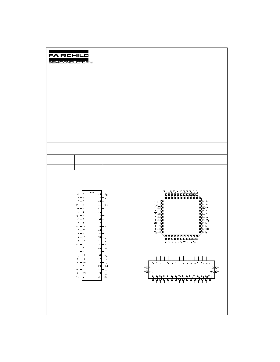
Connection Diagrams
Pin Assignment for SSOP
Pin Assignment for PLCC
Logic Symbol
Order Number
Package Number
Package Description
74FR16540QC
V44A
44-Lead Plastic Lead Chip Carrier (PLCC), JEDEC MO-047, 0.650 Square
74FR16540SSC
MS48A
48-Lead Small Shrink Outline Package (SSOP), JEDEC MO-118, 0.300 Wide

www.fairchildsemi.com
2
74FR16540
Pin Descriptions
Truth Table
H
=
HIGH Voltage Level
L
=
LOW Voltage Level
X
=
Immaterial
Z
=
High Impedance
Logic Diagram
Pin Names
Description
OE
n
Output Enable Inputs
I
0
≠I
15
Inputs
O
0
≠O
15
3-STATE Outputs
Inputs
Outputs
Byte1 [0:7] Byte2 [8:15]
I
0
≠I
7
I
8
≠I
15
O
0
≠O
7
O
8
≠O
15
OE
1
OE
2
OE
3
OE
4
L
L
L
L
H
H
L
L
H
X
L
L
X
L
Z
H
X
H
L
L
X
H
Z
L
L
L
H
X
L
X
H
Z
L
L
X
H
H
X
L
Z
H
H
H
H
X
X
Z
Z
L
L
L
L
L
L
H
H

3
www.fairchildsemi.com
7
4FR16540
Absolute Maximum Ratings
(Note 1)
Recommended Operating
Conditions
Note 1: Absolute maximum ratings are values beyond which the device
may be damaged or have its useful life impaired. Functional operation
under these conditions is not implied.
Note 2: Either voltage limit or current limit is sufficient to protect inputs.
DC Electrical Characteristics
Storage Temperature
-
65
∞
C to
+
150
∞
C
Ambient Temperature under Bias
-
55
∞
C to
+
125
∞
C
Junction Temperature under Bias
-
55
∞
C to
+
150
∞
C
V
CC
Pin Potential to Ground Pin
-
0.5V to
+
7.0V
Input Voltage (Note 2)
-
0.5V to
+
7.0V
Input Current (Note 2)
-
30 mA to
+
5.0 mA
Voltage Applied to Output
in HIGH State (with V
CC
=
0V)
Standard Output
-
0.5V to V
CC
3-STATE Output
-
0.5V to
+
5.5V
Current Applied to Output
in LOW State (Max)
Twice the Rated I
OL
(mA)
ESD Last Passing Voltage (Min)
4000V
Free Air Ambient Temperature
0
∞
C to
+
70
∞
C
Supply Voltage
+
4.5V to
+
5.5V
Symbol
Parameter
Min
Typ
Max
Units
V
CC
Conditions
V
IH
Input HIGH Voltage
2.0
V
Recognized as a HIGH Signal
V
IL
Input LOW Voltage
0.8
V
Recognized as a LOW Signal
V
CD
Input Clamp Diode Voltage
-
1.2
V
Min
I
IN
=
-
18 mA
V
OH
Output HIGH Voltage
2.4
V
Min
I
OH
=
-
3 mA
2.0
I
OH
=
-
15 mA
V
OL
Output LOW Voltage
0.55
V
Min
I
OL
=
64 mA
I
IH
Input HIGH Current
5.0
µ
A
Max
V
IN
=
2.7V
I
BVI
Input HIGH Current
7.0
µ
A
Max
V
IN
=
7.0V
Breakdown Test
(OE
n
)
I
IL
Input LOW Current
-
120
µ
A
Max
V
IN
=
0.5V
I
OS
Output Short-Circuit Current
-
100
-
225
mA
Max
V
OUT
=
0V
I
OZH
Output Leakage Current
0
20
µ
A
Max
V
OUT
=
2.7V
I
OZL
Output Leakage Current
0
-
20
µ
A
Max
V
OUT
=
0.5V
I
CEX
Output HIGH Leakage Current
50
µ
A
Max
V
OUT
=
V
CC
V
ID
Input Leakage Test
4.75
V
0.0
I
ID
=
1.9
µ
A
All Other Pins Grounded
I
OD
Output Circuit
3.75
µ
A
0.0
V
IOD
=
150 mV
Leakage Current
All Other Pins Grounded
I
ZZ
Bus Drainage Test
100
µ
A
0.0
V
OUT
=
5.25V
I
CCH
Power Supply Current
14
20
mA
Max
V
O
=
HIGH
I
CCL
Power Supply Current
75
92
mA
Max
V
O
=
LOW
I
CCZ
Power Supply Current
38
50
mA
Max
V
O
=
HIGH Z
C
IN
Input Capacitance
8
pF
5.0
www.fairchildsemi.com
4
74FR16540
AC Electrical Characteristics
Extended AC Characteristics
Note 3: Skew is defined as the absolute value of the difference between the actual propagation delays for any two outputs of the same device. The specifi-
cation applies to any outputs switching HIGH-to-LOW (t
OSHL
), LOW-to-HIGH, (t
OSLH
), or HIGH-to-LOW and/or LOW-to-HIGH, (t
OST
). Specifications guaran-
teed with all outputs switching in phase. This specification is guaranteed but not tested.
Note 4: This specification is guaranteed but not tested. The limits apply to propagation delays for all paths described switching in phase,
i.e., all LOW-to-HIGH, HIGH-to-LOW, 3-STATE-to-HIGH, etc.
Note 5: These specifications guaranteed but not tested. The limits represent propagation delays with 250 pF load capacitors in place of the 50 pF load
capacitors in the standard AC load. This specification pertains to single output switching only.
Symbol
Parameter
T
A
=
+
25
∞
C
T
A
=
0
∞
C to
+
70
∞
C
Units
V
CC
=
+
5.0V
V
CC
=
+
5.0V
C
L
=
50 pF
C
L
=
50 pF
Min
Typ
Max
Min
Max
t
PLH
Propagation Delay
1.0
2.8
4.3
1.0
4.3
ns
t
PHL
In to On
1.0
2.0
4.3
1.0
4.3
t
PZH
Output Enable Time
3.4
5.6
11.6
3.4
11.6
ns
t
PZL
3.4
7.8
11.6
3.4
11.6
t
PHZ
Output Disable Time
1.8
4.0
6.6
1.8
6.6
ns
t
PLZ
1.8
4.4
6.6
1.8
6.6
Symbol
Parameter
T
A
=
0
∞
C to
+
70
∞
C
T
A
=
0
∞
C to
+
70
∞
C
Units
V
CC
=
+
5.0V
V
CC
=
+
5.0V
C
L
=
50 pF
C
L
=
250 pF
16 Outputs Switching
(Note 4)
(Note 5)
Min
Max
Min
Max
t
PLH
Propagation Delay
1.0
6.0
3.2
8.2
ns
t
PHL
In to On
1.0
6.0
3.2
8.2
t
PZH
Output Enable Time
3.4
14.5
ns
t
PZL
3.4
14.5
t
PHZ
Output Disable Time
1.8
6.6
ns
t
PLZ
1.8
6.6
t
OSHL
Pin-to-Pin Skew
1.4
ns
(Note 3)
for HL Transitions
t
OSLH
Pin-to-Pin Skew
1.6
ns
(Note 3)
for LH Transitions
t
OST
Pin-to-Pin Skew
3.0
ns
(Note 3)
for HL/LH Transitions
5
www.fairchildsemi.com
7
4FR16540
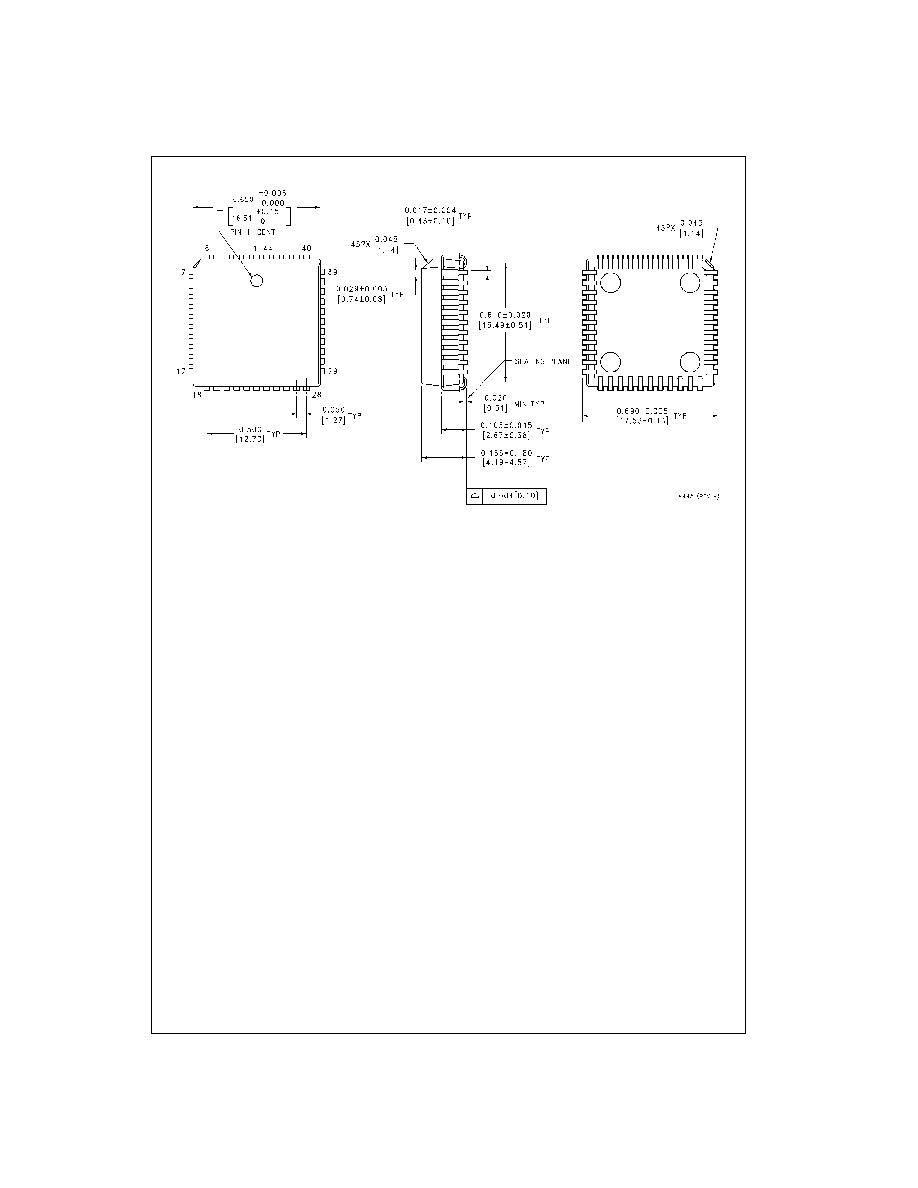
Physical Dimensions
inches (millimeters) unless otherwise noted
44-Lead Plastic Lead Chip Carrier (PLCC), JEDEC MO-047, 0.650 Square
Package Number V44A