©2002 Fairchild Semiconductor Corporation
Rev. A4, October 2002
KSH42C
PNP Epitaxial Silicon Transistor
Absolute Maximum Ratings
T
C
=25
°
C unless otherwise noted
Electrical Characteristics
T
C
=25
°
C unless otherwise noted
* Pulse Test: PW
300
µ
s, Duty Cycle
2%
Symbol
Parameter
Value
Units
V
CBO
Collector-Base Voltage
-100
V
V
CEO
Collector-Emitter Voltage
-100
V
V
EBO
Emitter-Base Voltage
-5
V
I
C
Collector Current (DC)
-6
A
I
CP
Collector Current (Pulse)
-10
A
I
B
Base Current
-2
A
P
C
Collector Dissipation (T
C
=25
°
C)
20
W
Collector Dissipation (T
a
=25
°
C)
1.75
W
T
J
Junction Temperature
150
°
C
T
STG
Storage Temperature
- 65 ~ 150
°
C
Symbol
Parameter
Test Condition
Min.
Max.
Units
V
CEO
(sus)
* Collector-Emitter Sustaining Voltage
I
C
= - 30mA, I
B
= 0
-100
V
I
CEO
Collector Cut-off Current
V
CE
= -60V, I
B
= 0
-50
µ
A
I
CES
Collector Cut-off Current
V
CE
= -100V, V
BE
= 0
-10
µ
A
I
EBO
Emitter Cut-off Current
V
BE
= -5V, I
C
= 0
-0.5
mA
h
FE
* DC Current Gain
V
CE
= -4V, I
C
= -0.3A
V
CE
= -4V, I
C
= -3A
30
15
75
V
CE
(sat)
* Collector-Emitter Saturation Voltage
I
C
= -6A, I
B
= -600mA
-1.5
V
V
BE
(on)
* Base-Emitter On Voltage
V
CE
= -6A, I
C
= -4A
-2
V
f
T
Current Gain Bandwidth Product
V
CE
= -10V, I
C
= -500mA
3
MHz
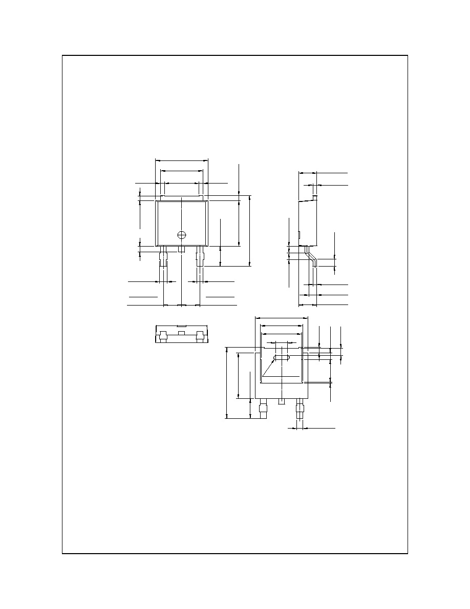
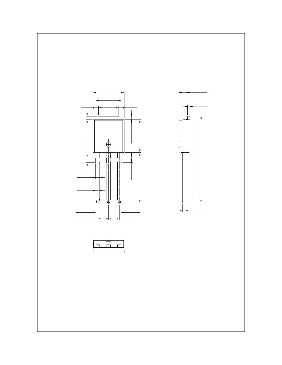
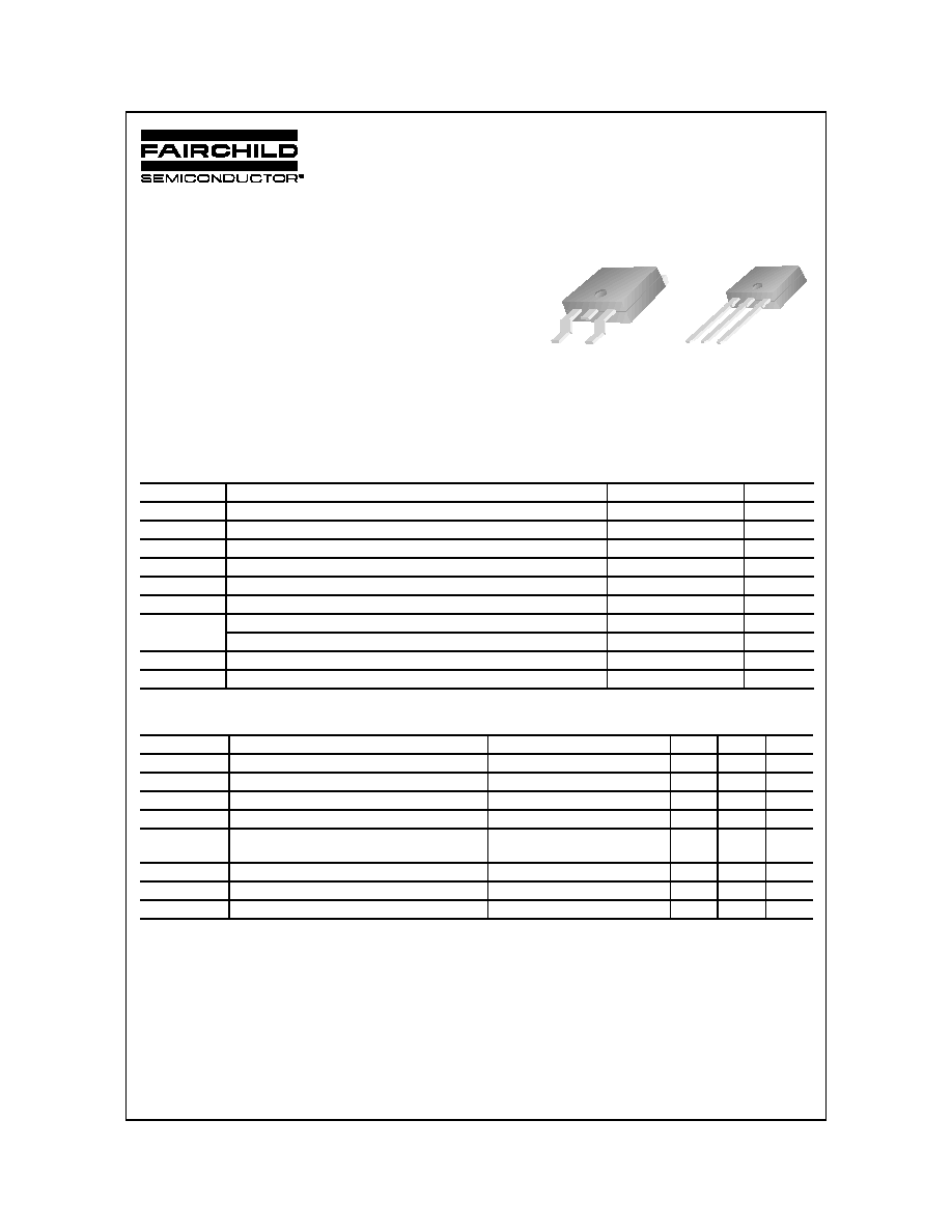
KSH42C
General Purpose Amplifier
Low Speed Switching Applications
· Lead Formed for Surface Mount Application (No Suffix)
· Straight Lead (I-PAK, "- I" Suffix)
· Electrically Similar to Popular TIP42C
1.Base 2.Collector 3.Emitter
D-PAK
I-PAK
1
1
©2002 Fairchild Semiconductor Corporation
Rev. A4, October 2002
KSH42C
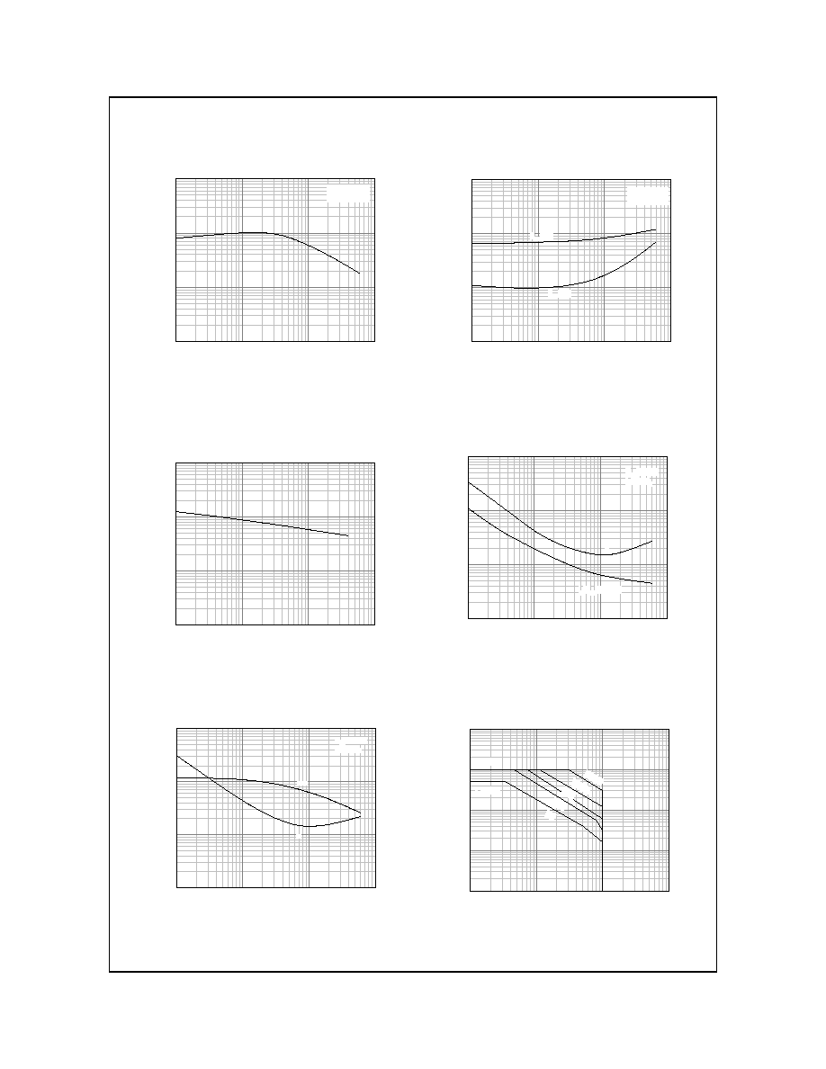
Typical Characteristics
Figure 1. DC current Gain
Figure 2. Base-Emitter Saturation Voltage
Collector-Emitter Saturation Voltage
Figure 3. Collector Capacitance
Figure 4. Turn On Time
Figure 5. Turn Off Time
Figure 6. Safe Operating Area
-0.01
-0.1
-1
-10
1
10
100
1000
V
CE
= -2V
h
FE
, DC C
URRENT
GAI
N
I
C
[A], COLLECTOR CURRENT
-0.01
-0.1
-1
-10
-0.01
-0.1
-1
-10
I
C
= 10 I
B
V
CE
(sat)
V
BE
(sat)
V
BE
(s
a
t
),
V
CE
(
s
at)
[
V
], S
A
T
URA
T
ION
V
O
LT
A
G
E
I
C
[A], COLLECTOR CURRENT
-0.1
-1
-10
-100
1
10
100
1000
C
ob
[pF
], C
A
P
A
CI
T
A
NCE
V
CB
[V], COLLECTOR-BASE VOLTAGE
-0.01
-0.1
-1
-10
0.01
0.1
1
10
t
R
V
CC
= -30V
I
C
= 10.I
B
t
D
V
BE
(off)=-5V
t
R
, t
D
[
µ
s], T
URN
ON
T
I
M
E
I
C
[A], COLLECTOR CURRENT
-0.01
-0.1
-1
-10
0.01
0.1
1
10
V
CC
= -30V
I
C
= 10.I
B
t
STG
t
F
t
ST
G
,t
F
[
µ
s], T
URN
O
F
F
T
I
M
E
I
C
[A], COLLECTOR CURRENT
-1
-10
-100
-1000
-0.01
-0.1
-1
-10
-100
5m
s
100
µ
s
500
µ
s
1m
s
DC
I
CP
(max)
I
C
(max)
I
C
[A], COL
L
ECT
O
R CURRENT
V
CE
[V], COLLECTOR-EMITTER VOLTAGE