 | –≠–ª–µ–∫—Ç—Ä–æ–Ω–Ω—ã–π –∫–æ–º–ø–æ–Ω–µ–Ω—Ç: L272 | –°–∫–∞—á–∞—Ç—å:  PDF PDF  ZIP ZIP |
©2001 Fairchild Semiconductor Corporation
www.fairchildsemi.com
Rev. 1.0.2
Features
∑ Output Current upto 0.7A
∑ Operates at Low Voltage (V
S(MIN)
=4V)
∑ Low Saturation Voltage (Ip=0.5A, V
O
=1.5V)
∑ Thermal Shutdown (TSD=160
∞
C)
∑ Ground Compatible Inputs
∑ Large Common mode & Differential mode Range
Applications
∑ Servo Amplifier
∑ Power Supply
∑ Compact Disc
∑ VCR
∑ Monitor
Description
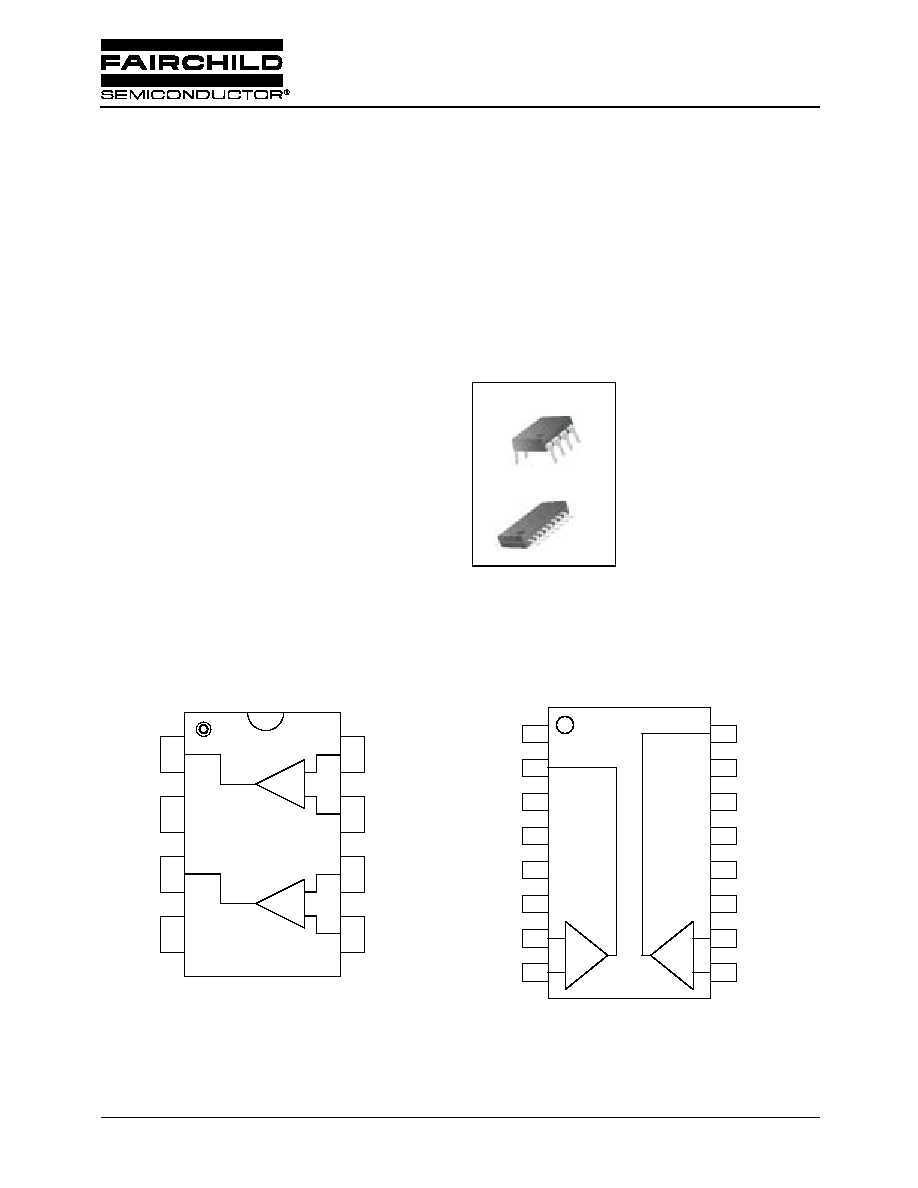
The L272 is a high-power dual operational amplifier
provided as a 8-DIP and 16-SOP package. The operational
amplifier is designed for low impedance loads and will
deliver output current upto 0.7A. The L272 can be used in a
wide range of applications including power supply, VCR,
monitor, servo amplifier, compact disc, etc
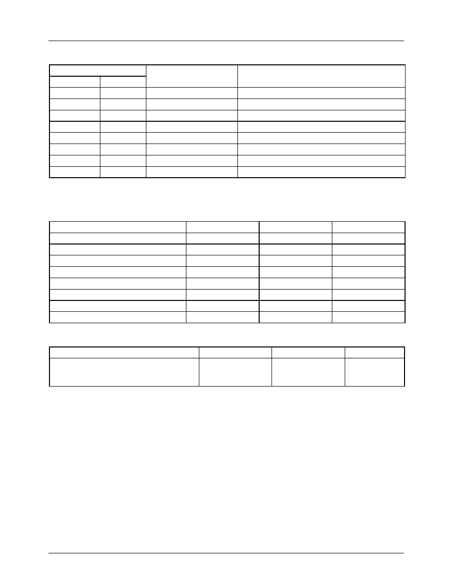
8-DIP
1
1
16-SOP
Internal Block Diagram
1
2
3
4
5
6
7
8
+
-
+
-
Vcc
V
EE
/GND
(8-DIP)
OUT1
OUT2
IN 1-
IN 1+
IN 2+
IN 2-
1
2
3
4
5
6
7
8
9
10
11
12
13
14
15
16
VCC
OUT2
VEE/GND
GND
IN2-
IN2+
IN1+
IN1-
GND
GND
OUT1
+
-
+
-
NC
NC
NC
NC
NC
1
2
3
4
5
6
7
8
9
10
11
12
13
14
15
16
VCC
OUT2
VEE/GND
GND
IN2-
IN2+
IN1+
IN1-
GND
GND
OUT1
+
-
+
-
NC
NC
NC
NC
NC
(16-SOP)
L272
Dual Power Operational Amplifier
L272
2
PIN Definitions
Absolute Maximum Ratings
Thermal Data
Pin Number
Pin Name
Pin Function Descrition
8-DIP
16-SOP
1
16
OUTPUT1
Amp Output 1
2
1
VCC
Positive Supply Voltage
3
2
OUTPUT2
Amp Output 2
4
4/5/12/13
VEE/GND
Negative Supply Voltage (GND)
5
7
INPUT-2
Amp Negative Input 2
6
8
INPUT+2
Amp Positive Input 2
7
9
INPUT+1
Amp Positive Input 1
8
10
INPUT-1
Amp Negative Input 1
Parameter
Symbol
Value
Unit
Supply Voltage
V
CC
40
V
Input Voltage
V
I
V
S
V
Differential Input Voltage
V
I(DIFF)
±
V
S
V
DC Output Current
I
O
0.7
A
Peak Output Current (non repetitive)
I
P
1
A
Power dissipation at: T
amb
=50
∞
C
P
tot
1
W
Operating Temperature Range
T
op
-25 to 85
∞
C
Storage and Junction Temperature
T
stg
, T
j
-40 to 150
∞
C
Parameter
Symbol
Value
Unit
Thermal Resistance Junction-Ambient Max.
8-DIP
16-SOP
R
ja
100
190
∞
C/W
L272
3
Electrical Characteristics
( Vcc = +12V, V
EE
= -12V, Ta = 25
∞
C unless otherwise specified )
Note :
1. Guaranteed by design. Not 100% tested in production.
Parameter
Symbol
Conditions
Min.
Typ.
Max.
Unit
Supply Voltage (V
CC
- V
EE
)
V
S
4
-
28
V
Supply Current
I
S
V
O
= V
CC
/2
V
CC
=24V, V
EE
=0V
V
CC
=12V, V
EE
=0V
-
8
7.5
12
11
mA
mA
Input Bias Current
I
BIAS
-
-
0.3
2.5
µ
A
Input Offset Voltage
V
IO
-
-
15
60
mV
Input Offset Current
I
IO
-
-
50
250
nA
Slew Rate
SR
Vin = 1Vpp, Unit Gain
-
1
-
V/
µ
s
Gain-Bandwidth Product
GBW
-
-
350
-
KHz
Input Resistance
R
I
-
500
-
-
K
Lange Signal
G
V
V
O(pp)
=
±
10V
65
75
-
dB
Input Noise Voltage
e
N
B = 20KHz
-
10
-
µ
V
Input Noise Current
I
N
B = 20KHz
-
200
-
pA
Common Mode Rejection Ratio
CMRR
-
60
75
-
dB
Supply Voltage Rejection Ratio
PSRR
V
CC
=+15V, V
EE
= -15V
V
CC
=+5V, V
EE
= -5V
54
62
-
dB
Output Voltage Swing
V
O
V
CC
= 24V, V
EE
= 0V
Ip = 0.1A
Ip = 0.5A
21
21
23
22.5
-
-
V
V
Channel Separation
C
S
f = 1kHz; R
L
= 10
,
G
V
= 30dB
-
60
-
dB
Total Harmonic Distortion
THD
f = 1kHz, G
V
= 1dB,R
L
=
-
0.5
-
%
Thermal stutdown Temperature
(Note1)
TSD
-
-
160
-
∞
C
L272
4
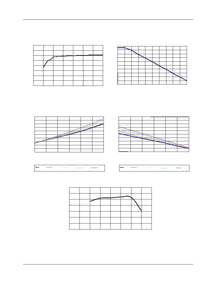
Typical Perfomance Characteristics
5
6
7
8
9
0
4
8
12
16
20
24
28
VCC/VEE/Supply Voltage(V)
Is
,S
upp
l
y
C
u
r
r
ent(
m
A
)
5
6
7
8
9
0
4
8
12
16
20
24
28
VCC/VEE/Supply Voltage(V)
Is
,S
upp
l
y
C
u
r
r
ent(
m
A
)
-20
0
20
40
60
80
1.E+01
1.E+02
1.E+03
1.E+04
1.E+05
1.E+06
f, Frequency(Hz)
Ga
in
(d
B)
-20
0
20
40
60
80
1.E+01
1.E+02
1.E+03
1.E+04
1.E+05
1.E+06
f, Frequency(Hz)
Ga
in
(d
B)
-12
-11
100
200
300
400
500
600
700
IL, Load Current (mA)
O
u
t
p
ut
V
o
l
t
ag
e S
w
i
ng (
V
)
0
25
50
75
100
-12
-11
100
200
300
400
500
600
700
IL, Load Current (mA)
O
u
t
p
ut
V
o
l
t
ag
e S
w
i
ng (
V
)
0
25
50
75
100
0
25
50
75
100
10.5
11
11.5
100
200
300
400
500
600
700
IL, Load Current (mA)
O
u
tpu
t
V
o
l
t
age
Swi
n
g
(
V
)
0
25
50
75
100
10.5
11
11.5
100
200
300
400
500
600
700
IL, Load Current (mA)
O
u
tpu
t
V
o
l
t
age
Swi
n
g
(
V
)
10.5
11
11.5
100
200
300
400
500
600
700
IL, Load Current (mA)
O
u
tpu
t
V
o
l
t
age
Swi
n
g
(
V
)
0
25
50
75
100
0
25
50
75
100
Figure 1. Supply Voltage vs Supply
Current with No Load
Figure 2. Open Loop Voltage Gain
Figure 3-1. Output Voltage Swing vs Load Current
Figure 3-2. Output Voltage Swing vs Load Current
0
20
40
60
1.E+01
5.E+01
1.E+02
5.E+02
1.E+03
5.E+03
1.E+04
5.E+04
1.E+05
f,Frequency(Hz)
CS(dB
)
0
20
40
60
1.E+01
5.E+01
1.E+02
5.E+02
1.E+03
5.E+03
1.E+04
5.E+04
1.E+05
f,Frequency(Hz)
CS(dB
)
Figure 6. Channel Separation vs Frepuency
L272
5
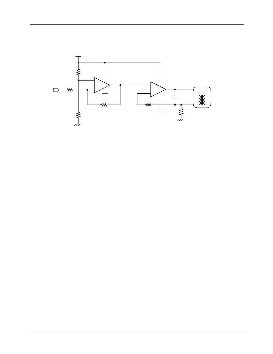
Applications
< Tilt Coil Current Control Circuit in Monitor, 8-DIP Package>
Tilt Coil
33
V
EE
3.3uF
50V
1
2
3
8
7
+
-
CH1
4
1k
CH2
+
-
V
EE
40k
9.1k
10k
36k
V
CC
2
4
6
5
IN