 | –≠–ª–µ–∫—Ç—Ä–æ–Ω–Ω—ã–π –∫–æ–º–ø–æ–Ω–µ–Ω—Ç: LM319N | –°–∫–∞—á–∞—Ç—å:  PDF PDF  ZIP ZIP |
©2001 Fairchild Semiconductor Corporation
www.fairchildsemi.com
Rev. 1.0.2
Features
∑ Operates from a single 5V supply
∑ Typically 80ns response time at
±
15V
∑ Open collector outputs : up to + 35V
∑ High output drive current : 25mA
∑ Inputs and outputs can be isolated from system ground
∑ Minimum fan-out of 2 (each side)
∑ Two independent comparators
Description
The LM319 is a dual high speed voltage comparator
designed to operate from a single + 5V supply up to ±15V
dual supplies. Open collector of the output stage makes the
LM319 compatible with RTL, DTL and TTL as well as
capable of driving lamps and relays at currents up to
25mA. Typical response time of 80ns with ±15V power
supplies makes the LM319 ideal for application in fast A/D
converts, level shifters, oscillators, and multivibrators.
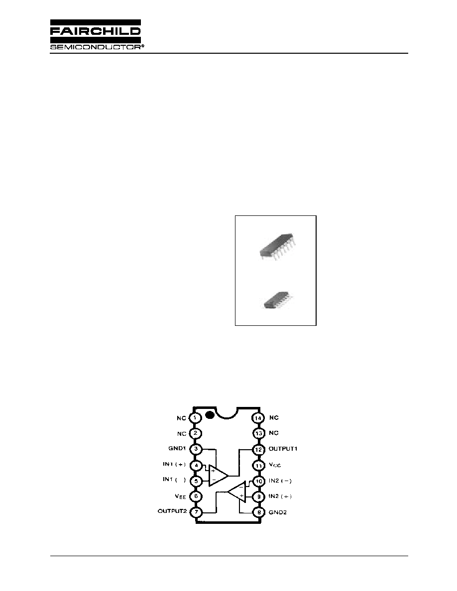
14-SOP
14-DIP
1
1
Internal Block Diagram
LM319
Dual Comparator
LM319
2
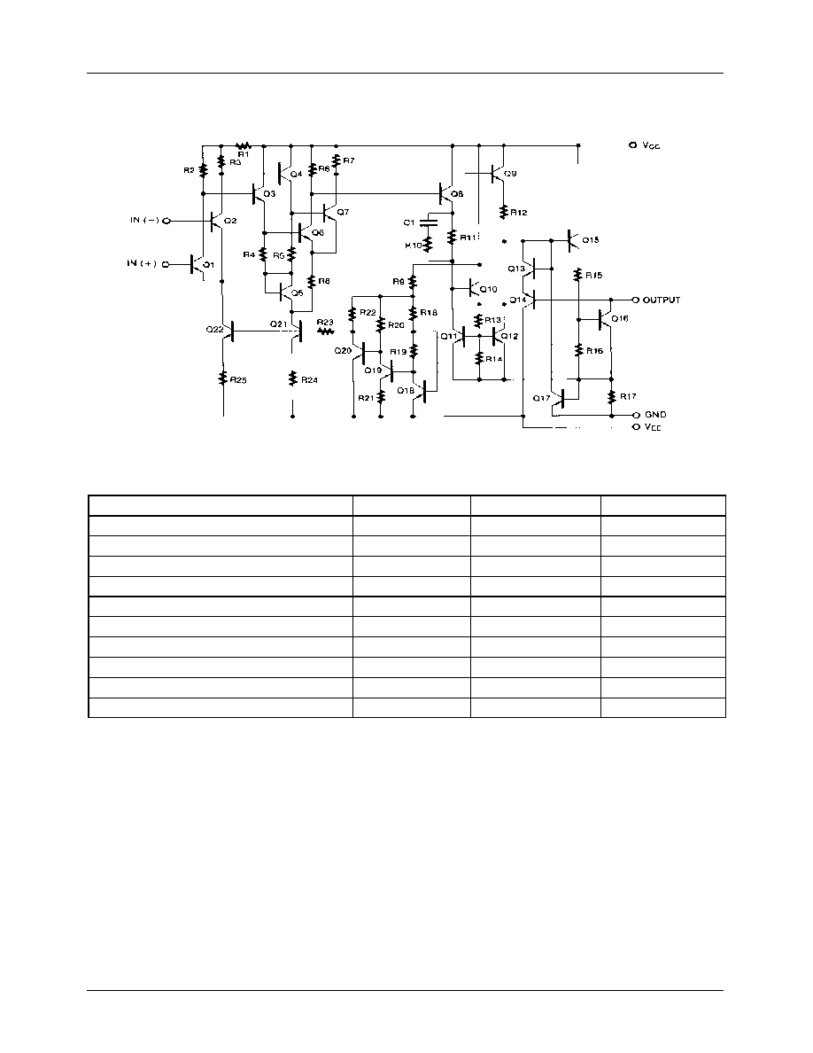
Schematic Diagram
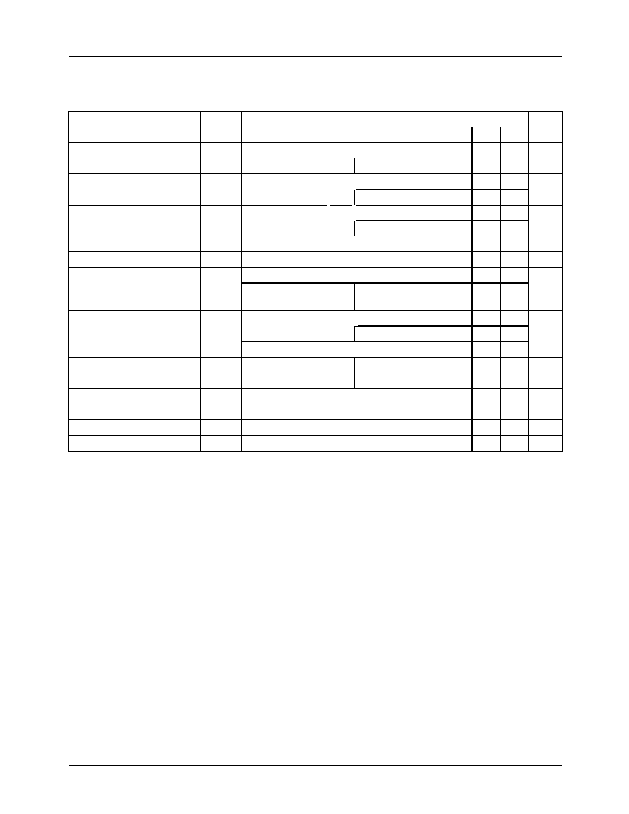
Absolute Maximum Ratings
Parameter
Symbol
Value
Unit
Supply Voltage
V
CC
36
V
Output to Negative Supply Voltage
V
O
- V
EE
36
V
Ground to Negative Supply Voltage
V
EE
25
V
Ground to Positive Supply Voltage
V
CC
18
V
Differential Input Voltage
V
I(DIFF)
5
V
Input Voltage
V
I
±
15
V
Output Short Circuit Duration
-
10
sec
Power Dissipation
P
D
500
mW
Operating Temperature Range
T
OPR
0 ~ + 70
∞
C
Storage Temperature Range
T
STG
-65 ~ + 150
∞
C
LM319
3
Electrical Characteristics
(V
CC
= + 15V, V
EE
= - 15V, T
A
= 25
∞
C, unless otherwise specified)
Notes :
1. The offset voltage and offset currents given are the maximum values required to drive the output within a volt of either
supply with a 1mA load. Thus, these parameters define an error band and take into account the worst case effects of
voltage gain and input impedance.
2. The response time specified is for a 100mV input step with 5mV overdrive.
3. LM319 : 0
T
A
+70
∞
C
Parameter
Symbol
Conditions
LM319
Unit
Min. Typ. Max.
Input Offset Voltage (Note 1)
V
IO
R
S
5K
-
2.0
8.0
mV
Note 3
-
-
10
Input Offset Current (Note 1)
I
IO
-
10
200
nA
Note 3
-
-
300
Input Bias Current
I
BIAS
-
150 1000
nA
Note 3
-
-
1200
Voltage Gain
G
V
-
8
40
-
V/mV
Response Time (Note 2)
T
RES
V
CC
=
±
15V
-
80
-
ns
Saturation Voltage
V
SAT
V
CC
=15V, V
EE
= -15V , V
I
-5mV, I
O
= 25mA
-
0.6
1.5
V
V
CC
= 4.5V,V
EE
= 0V
V
I
-10mV, I
O
3.2mA
Note3
-
0.3
0.4
Output Leakage Current
I
O(LKG)
V
I
5mV, V
O(P)
= 35V
-
-
-
µ
A
Note 3
-
-
-
V
I
10mV, V
O(P)
= 35V
-
0.2
10
Input Voltage Range
V
I(R)
Note 3
V
CC
=
±
15V
-
±
13
-
V
V
CC
= 5V, V
EE
= 0V
1
-
3
Differential Input Voltage
V
I(DIFF)
-
-
-
±
5
V
Positive Supply Current
I
CC1
V
CC
= 5V, V
EE
= 0V
-
3.6
-
mA
Positive Supply Current
I
CC2
V
CC
=
±
15V
-
7.5
12.5
mA
Negative Supply Current
I
EE
V
CC
=
±
15V
-
3
5
mA
LM319
4
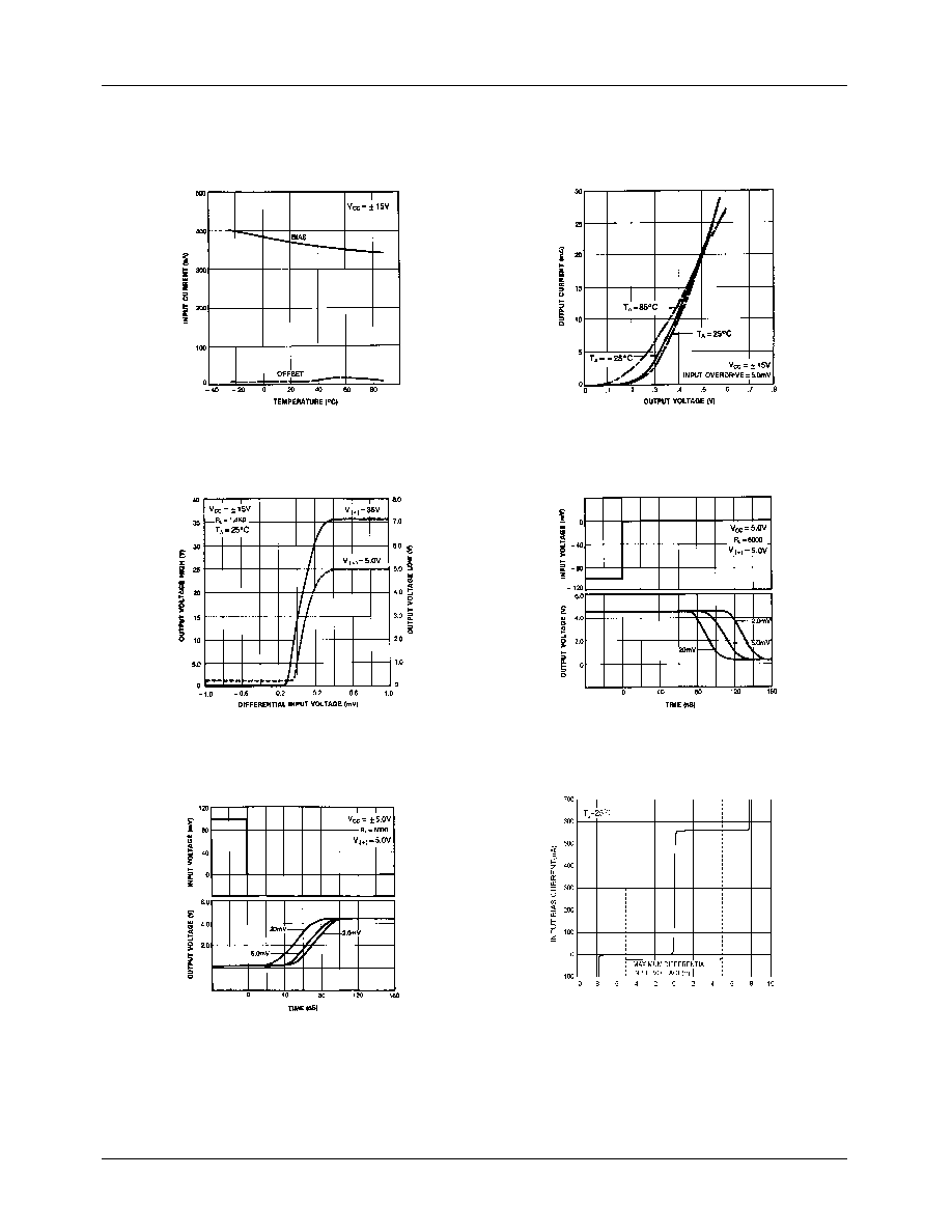
Typical Performance Characteristics
Figure 1. Input Current
Figure 2. Output Saturation Voltage
Figure 3. Transfer Function
Figure 4. Response Time for Various Input Overdriver
Figure 5. Response Time Various Input Overdriver
Figure 6. Input Characteristics
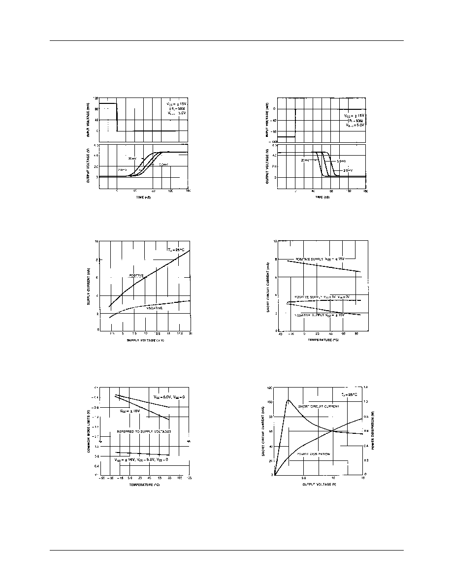
LM319
5
Typical Performance Characteristics (continued)
Figure 7. Response Time for Various Input Overdriver
Figure 8. Response Time for Various Input Overdriver
Figure 9. Supply Current
Figure 10. Supply Current
Figure 11. Common Mode Limits
Figure 12. Output Limiting Characteristics