 | –≠–ª–µ–∫—Ç—Ä–æ–Ω–Ω—ã–π –∫–æ–º–ø–æ–Ω–µ–Ω—Ç: LM348 | –°–∫–∞—á–∞—Ç—å:  PDF PDF  ZIP ZIP |
©2001 Fairchild Semiconductor Corporation
www.fairchildsemi.com
Rev. 1.0.1
Features
∑ LM741 OP Amp operating characteristics
∑ Low supply current drain
∑ Class AB output stage no crossover distortion
∑ Pin compatible with the LM324/LM248
∑ Low input offset voltage : 1mV Typ.
∑ Low input offset current : 4nA Typ.
∑ Low input bias current : 30nA Typ.
∑ Gain bandwidth (unity gain): 1.0MHz Typ.
∑ High degree of isolation between amplifiers: 120dB
∑ Overload protection for inputs and outputs
Description
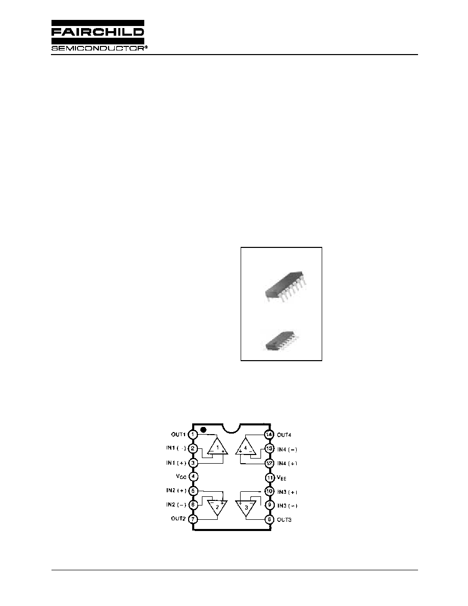
TheLM348/LM248 is a true quad LM741. It consists of four
independent, high-gain, internally compensated, low power
operational amplifiers which have been designed to provide
functional characteristics identical to those of the familiar
LM741 operational amplifier. In addition the total supply
current for all four amplifiers is comparable to the supply
current of a single LM741 type OP Amp. Other features
include input offset currents and input bias current which are
much less than those of a standard LM741. Also, excellent
isolation between amplifiers has been achieved by
independently biasing each amplifier and using layout
techniques which minimize thermal coupling.
14-DIP
1
14-SOP
1
Internal Block Diagram
LM348/LM248
Quad Operational Amplifier
LM348/LM248
2
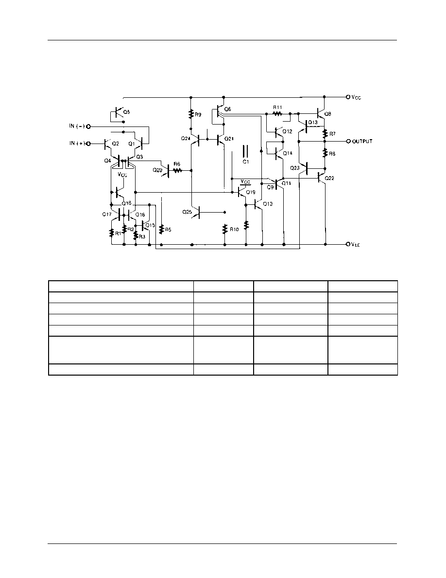
Schematic Diagram
(One Section Only)
Absolute Maximum Ratings
Parameter
Symbol
Value
Unit
Supply Voltage
V
CC
±
18
V
Differential Input Voltage
V
I(DIFF)
36
V
Input Voltage
V
I
±
18
V
Output Short Circuit Duration
-
Continuous
-
Operating Temperature
LM348
LM248
T
OPR
0 ~ +70
-25 ~ +85
∞
C
Storage Temperature
T
STG
- 65~ +150
∞
C
LM348/LM248
3
Electrical Characteristics
(V
CC
=15V, V
EE
= -15V, T
A
=25
∞
C, unless otherwise specified)
Note :
1. LM348: 0
T
A
+70
∞
C , LM248: -25
T
A
+85
∞
C
2. Guaranteed by design.
Parameter Symbol
Conditions
LM248
LM348
Unit
Min. Typ. Max. Min. Typ. Max.
Input Offset Voltage
V
IO
R
S
10K
-
1
6.0
-
1
6.0
mV
Note 1
-
-
7.5
-
-
7.5
Input Offset Current
I
IO
-
4
50
-
4
50
nA
Note 1
-
-
125
-
-
100
Input Bias Current
I
BIAS
-
30
200
-
30
200
nA
Note 1
-
-
500
-
-
400
Input Resistance
R
I
-
0.8
2.5
-
0.8
2.5
-
M
Supply Current (all Amplifiers)
I
CC
-
-
2.4
4.5
-
2.4
4.5
mA
Large Signal Voltage Gain
G
V
R
L
2K
25
160
-
25
160
-
V/mV
Note 1
15
-
-
15
-
-
Channel Separation
CS
f = 1KHz to 20KHz
-
120
-
-
120
-
dB
Common Mode Input
Voltage Range
V
I(R)
Note 1
±
12
-
-
±
12
-
-
V
Small Signal Bandwidth
BW
G
V
= 1
-
1.0
-
-
1.0
-
MHz
Phase Margin (Note2)
MPH
G
V
= 1
-
60
-
-
60
-
Degree
Slew Rate (Note2)
SR
G
V
= 1
-
0.5
-
-
0.5
-
V/
µ
s
Output Short Circuit Current
I
SC
-
-
25
-
-
25
-
mA
Output Voltage Swing
V
O(P-P)
R
L
10K
Note 1
±
12
±
13
-
±
12
±
13
-
V
R
L
2K
±
10
±
12
-
±
10
±
12
-
Common Mode Rejection
Ratio
CMRR
R
S
10K
Note 1
70
90
-
70
90
-
dB
Power Supply Rejection Ratio
PSRR
R
S
10K
Note 1
77
96
-
77
96
-
dB
LM348/LM248
4
Typical Performance Characteristics
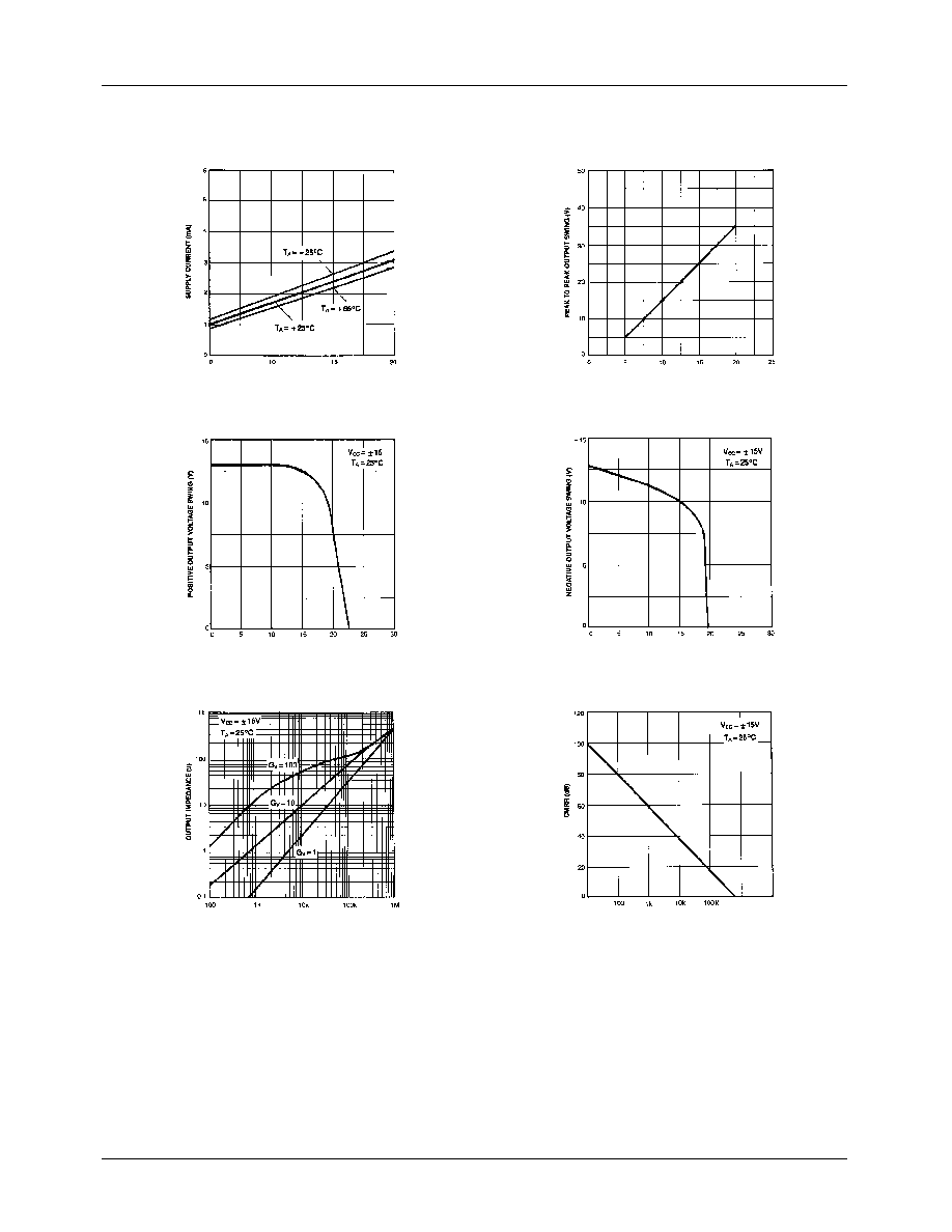
Figure 1. Supply Current vs Supply voltage
Figure 2. Output Voltage Swing vs Supply voltage
Figure 3. Output voltage swing vs Source Current (mA)
Figure 4. Output voltage swing vs Sink Current (mA)
Figure 5. Output Impedance vs Frequency
Figure 6. Common-mode Rejection Ratio vs Frequency
Supply Voltage (V)
Supply Voltage (V)
Source Current (mA)
Sink Current (mA)
Frequency (Hz)
Frequency (Hz)
LM348/LM248
5
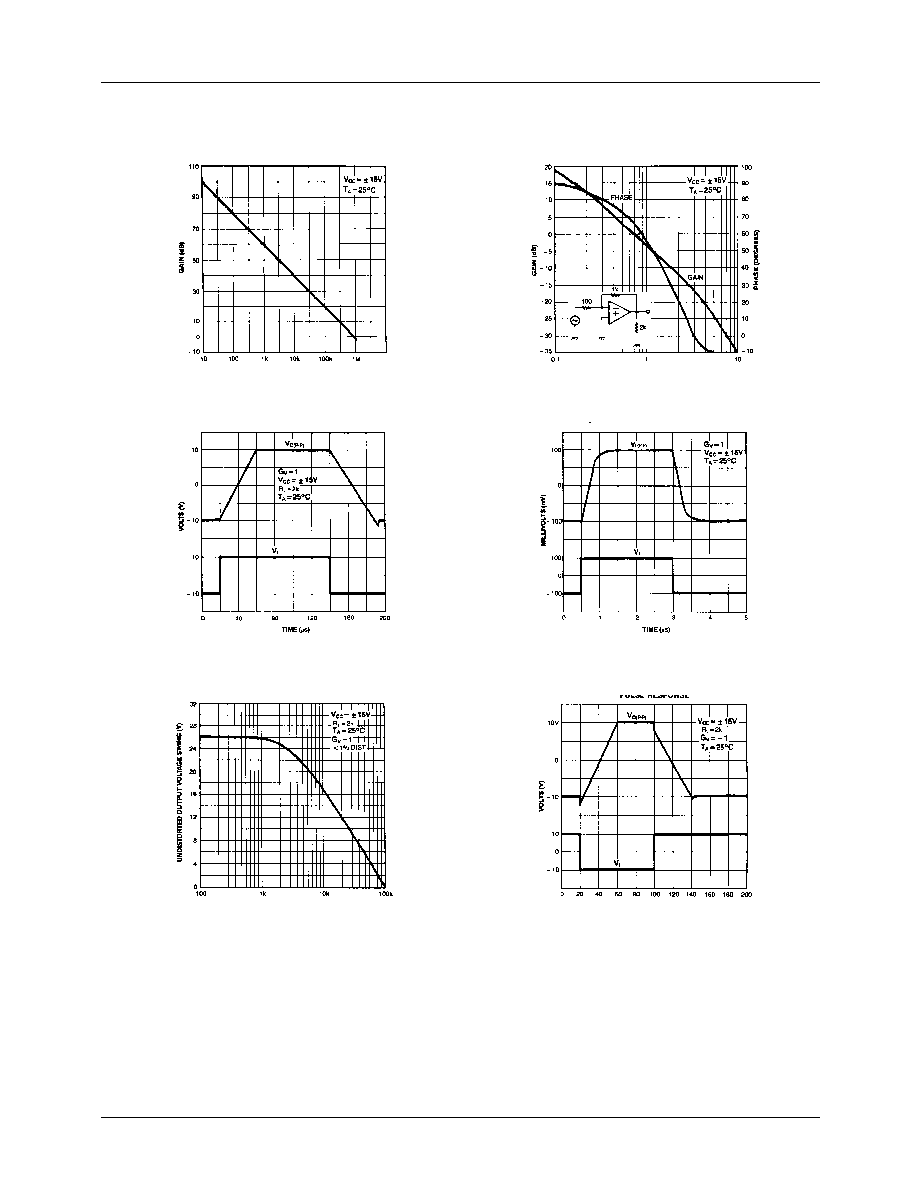
Typical Performance Characteristics (continued)
Figure 7. Open Loop Frequency Response
Figure 8. Bode Plot
Figure 9. Large Signal Pulse Response
Figure 10. Small Signal Pulse Response
Figure 11. Undistorted Output Voltage Swing vs Frequency
Figure 12. Inverting Large Signal Pulse Response