 | –≠–ª–µ–∫—Ç—Ä–æ–Ω–Ω—ã–π –∫–æ–º–ø–æ–Ω–µ–Ω—Ç: LM358N | –°–∫–∞—á–∞—Ç—å:  PDF PDF  ZIP ZIP |
©2002 Fairchild Semiconductor Corporation
www.fairchildsemi.com
Rev. 1.0.2
Features
∑ Internally Frequency Compensated for Unity Gain
∑ Large DC Voltage Gain: 100dB
∑ Wide Power Supply Range:
LM258/LM258A, LM358/LM358A: 3V~32V (or ±1.5V
~ 16V)
LM2904 : 3V~26V (or ±1.5V ~ 13V)
∑ Input Common Mode Voltage Range Includes Ground
∑ Large Output Voltage Swing: 0V DC to Vcc -1.5V DC
∑ Power Drain Suitable for Battery Operation.
Description
The LM2904,LM358/LM358A, LM258/LM258A consist of
two independent, high gain, internally frequency
compensated operational amplifiers which were designed
specifically to operate from a single power supply over a
wide range of voltage. Operation from split power supplies
is also possible and the low power supply current drain is
independent of the magnitude of the power supply voltage.
Application areas include transducer amplifier, DC gain
blocks and all the conventional OP-AMP circuits which now
can be easily implemented in single power supply systems.
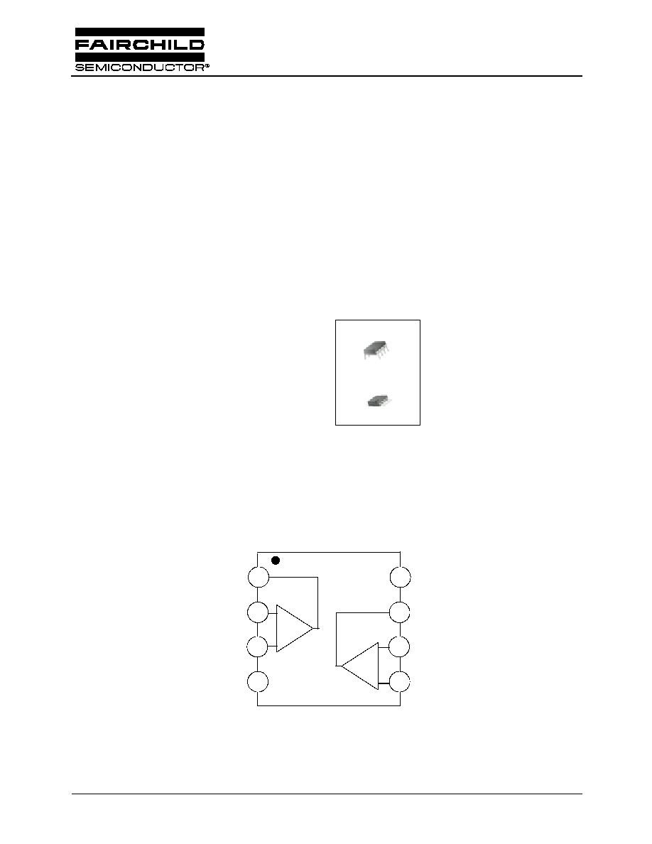
8-DIP
8-SOP
1
1
Internal Block Diagram
-
+
+
-
1
2
3
4
5
6
7
8 V
CC
OUT2
IN2 (-)
IN2 (+)
OUT1
IN1 (-)
IN1 (+)
GND
LM2904,LM358/LM358A,LM258/
LM258A
Dual Operational Amplifier
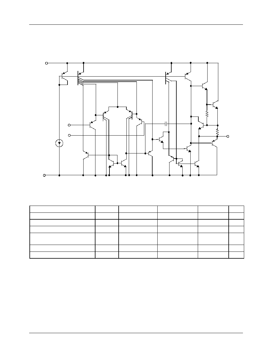
LM2904,LM358/LM358A,LM258/LM258A
2
Schematic Diagram
(One section only)
Absolute Maximum Ratings
Parameter
Symbol
LM258/LM258A
LM358/LM358A
LM2904
Unit
Supply Voltage
V
CC
±
16 or 32
±
16 or 32
±
13 or 26
V
Differential Input Voltage
V
I(DIFF)
32
32
26
V
Input Voltage
V
I
-0.3 to +32
-0.3 to +32
-0.3 to +26
V
Output Short Circuit to GND
V
CC
15V, T
A
= 25
∞
C(One Amp)
-
Continuous
Continuous
Continuous
-
Operating Temperature Range
T
OPR
-25 ~ +85
0 ~ +70
-40 ~ +85
∞
C
Storage Temperature Range
T
STG
-65 ~ +150
-65 ~ +150
-65 ~ +150
∞
C
Q8
Q7
Q6
Q5
Q4
Q3
Q2
Q1
Q9
Q10
Q11
Q12
Q14
Q15
Q16
Q18
Q19
Q20
R2
Q21
C1
R1
GND
OUTPUT
IN(+)
IN(-)
V
CC
Q13
Q17
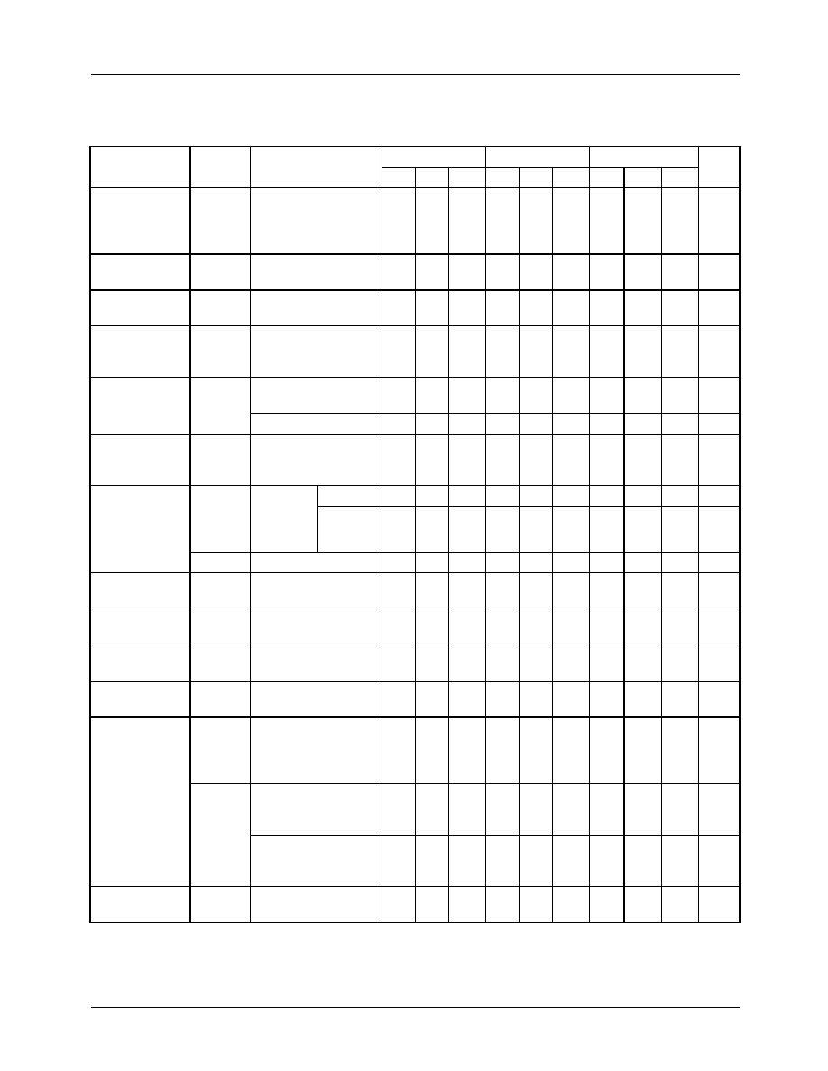
LM2904,LM358/LM358A,LM258/LM258A
3
Electrical Characteristics
(Vcc = 5.0V, V
EE
= GND, T
A
= 25
∞
C, unless otherwise specified)
Note:
1. This parameter, although guaranteed, is not 100% tested in production.
Parameter Symbol
Conditions
LM258
LM358
LM2904
Unit
Min. Typ. Max. Min. Typ. Max. Min. Typ. Max.
Input Offset
Voltage
V
IO
V
CM
= 0V to V
CC
-1.5V
V
O(P)
= 1.4V,
R
S
= 0
-
2.9
5.0
-
2.9
7.0
-
2.9
7.0
mV
Input Offset
Current
I
IO
-
-
3
30
-
5
50
-
5
50
nA
Input Bias
Current
I
BIAS
-
-
45
150
-
45
250
-
45
250
nA
Input Voltage
Range
V
I(R)
V
CC
= 30V
(LM2904, V
CC
=26V)
0
-
Vcc
-1.5
0
-
Vcc
-1.5
0
-
Vcc
-1.5
V
Supply Current
I
CC
R
L
=
, V
CC
= 30V
(LM2904, V
CC
=26V)
-
0.8
2.0
-
0.8
2.0
-
0.8
2.0
mA
R
L
=
, V
CC
= 5V
-
0.5
1.2
-
0.5
1.2
-
0.5
1.2
mA
Large Signal
Voltage Gain
G
V
V
CC
= 15V,
R
L
=
2k
V
O(P)
= 1V to 11V
50
100
-
25
100
-
25
100
-
V/mV
Output Voltage
Swing
V
O(H)
V
CC
=30V
(V
CC
=26V for
LM2904)
R
L
= 2k
26
-
-
26
-
-
22
-
-
V
R
L
=
10k
27
28
-
27
28
-
23
24
-
V
V
O(L)
V
CC
= 5V, R
L
=
10k
-
5
20
-
5
20
-
5
20
mV
Common-Mode
Rejection Ratio
CMRR
-
70
85
-
65
80
-
50
80
-
dB
Power Supply
Rejection Ratio
PSRR
-
65
100
-
65
100
-
50
100
-
dB
Channel
Separation
CS
f = 1kHz to 20kHz
(Note1)
-
120
-
-
120
-
-
120
-
dB
Short Circuit to
GND
I
SC
-
-
40
60
-
40
60
-
40
60
mA
Output Current
I
SOURCE
V
I(+)
= 1V,
V
I(-)
= 0V
V
CC
= 15V,
V
O(P)
= 2V
20
30
-
20
30
-
20
30
-
mA
I
SINK
V
I(+)
= 0V, V
I(-)
= 1V,
V
CC
= 15V,
V
O(P)
= 2V
10
15
-
10
15
-
10
15
-
mA
V
I(+)
= 0V,V
I(-)
=1V ,
V
CC
= 15V,
V
O(P)
= 200mV
12
100
-
12
100
-
-
-
-
µ
A
Differential
Input Voltage
V
I(DIFF)
-
-
-
V
CC
-
-
V
CC
-
-
V
CC
V
LM2904,LM358/LM358A,LM258/LM258A
4
Electrical Characteristics
(Continued)
(V
CC
= 5.0V, V
EE
= GND, unless otherwise specified)
The following specification apply over the range of -25
∞
C
T
A
+85
∞
C for the LM258; and the 0
∞
C
T
A
+70
∞
C
for the LM358; and the -40
∞
C
T
A
+85
∞
C for the LM2904
Parameter
Symbol
Conditions
LM258
LM358
LM2904
Unit
Min. Typ. Max. Min. Typ. Max. Min. Typ. Max.
Input Offset
Voltage
V
IO
V
CM
= 0V to
V
CC
-1.5V
V
O(P)
= 1.4V,
R
S
= 0
-
-
7.0
-
-
9.0
-
-
10.0
mV
Input Offset
Voltage Drift
V
IO/
T
R
S
= 0
-
7.0
-
-
7.0
-
-
7.0
-
µ
V/
∞
C
Input Offset
Current
I
IO
-
-
-
100
-
-
150
-
45
200
nA
Input Offset
Current Drift
I
IO
/
T
-
-
10
-
-
10
-
-
10
-
pA/
∞
C
Input Bias
Current
I
BIAS
-
-
40
300
-
40
500
-
40
500
nA
Input Voltage
Range
V
I(R)
V
CC
= 30V
(LM2904 ,
V
CC
= 26V)
0
-
Vcc
-2.0
0
-
Vcc
-2.0
0
-
Vcc
-2.0
V
Large Signal
Voltage Gain
G
V
V
CC
= 15V,
R
L
=
2.0k
V
O(P)
= 1V to 11V
25
-
-
15
-
-
15
-
-
V/mV
Output Voltage
Swing
V
O(H)
V
CC
=30V
(V
CC
=
26V for
LM2904)
R
L
= 2k
26
-
-
26
-
-
22
-
-
V
R
L
=10k
27
28
-
27
28
-
23
24
-
V
V
O(L)
V
CC
= 5V, R
L
=
10k
-
5
20
-
5
20
-
5
20
mV
Output Current
I
SOURCE
V
I(+)
= 1V,
V
I(-)
= 0V
V
CC
= 15V,
V
O(P)
= 2V
10
30
-
10
30
-
10
30
-
mA
I
SINK
V
I(+)
= 0V,
V
I(-)
= 1V
V
CC
= 15V,
V
O(P)
= 2V
5
8
-
5
9
-
5
9
-
mA
Differential
Input Voltage
V
I(DIFF)
-
-
-
V
CC
-
-
V
CC
-
-
V
CC
V

LM2904,LM358/LM358A,LM258/LM258A
5
Electrical Characteristics
(Continued)
(V
CC
= 5.0V, V
EE
= GND, T
A
= 25
∞
C, unless otherwise specified)
Note:
1. This parameter, although guaranteed, is not 100% tested in production.
Parameter Symbol
Conditions
LM258A
LM358A
Unit
Min. Typ.
Max. Min. Typ.
Max.
Input Offset Voltage
V
IO
V
CM
= 0V to V
CC
-1.5V
V
O(P)
= 1.4V, R
S
= 0
-
1.0
3.0
-
2.0
3.0
mV
Input Offset Current
I
IO
-
-
2
15
-
5
30
nA
Input Bias Current
I
BIAS
-
-
40
80
-
45
100
nA
Input Voltage Range
V
I(R)
V
CC
= 30V
0
-
V
CC
-1.5
0
-
V
CC
-1.5
V
Supply Current
I
CC
R
L
=
,V
CC
= 30V
-
0.8
2.0
-
0.8
2.0
mA
RL =
, V
CC
= 5V
-
0.5
1.2
-
0.5
1.2
mA
Large Signal Voltage
Gain
G
V
V
CC
= 15V, R
L
=
2k
V
O
= 1V to 11V
50
100
-
25
100
-
V/mV
Output Voltage Swing
V
OH
V
CC
= 30V
R
L
= 2k
26
-
-
26
-
-
V
R
L
=10k
27
28
-
27
28
-
V
V
O(L)
V
CC
= 5V, R
L
=
10k
-
5
20
-
5
20
mV
Common-Mode
Rejection Ratio
CMRR
-
70
85
-
65
85
-
dB
Power Supply
Rejection Ratio
PSRR
-
65
100
-
65
100
-
dB
Channel Separation
CS
f = 1kHz to 20kHz (Note1)
-
120
-
-
120
-
dB
Short Circuit to GND
I
SC
-
-
40
60
-
40
60
mA
Output Current
I
SOURCE
V
I(+)
= 1V, V
I(-)
= 0V
V
CC
= 15V, V
O(P)
= 2V
20
30
-
20
30
-
mA
I
SINK
V
I(+)
= 1V, V
I(-)
= 0V
V
CC
= 15V, V
O(P)
= 2V
10
15
-
10
15
-
mA
V
in +
= 0V, V
in (-)
= 1V
V
O(P)
= 200mV
12
100
-
12
100
-
µ
A
Differential Input
Voltage
V
I(DIFF)
-
-
-
V
CC
-
-
V
CC
V