©2002 Fairchild Semiconductor Corporation
www.fairchildsemi.com
Rev. 1.0.3
Features
∑ Programmable Output Voltage to 36 Volts
∑ Low Dynamic Output Impedance 0.20 Typical
∑ Sink Current Capability of 1.0 to 100mA
∑ Equivalent Full-Range Temperature Coefficient of
50ppm/
∞
C Typical
∑ Temperature Compensated for Operation Over Full Rated
Operating Temperature Range
∑ Low Output Noise Voltage
∑ Fast Turn-on Response
Description
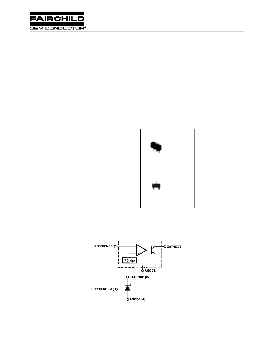
The LM431SA/LM431SB/LM431SC are three terminal
output adjustable regulators with thermal stability over
operating temperature range. The output voltage can be set
any value between V
REF
(approximately 2.5 volts) and 36
volts with two external resistors. These devices have a
typical dynamic output impedance of 0.2
Active output
circuit provides a sharp turn-on characteristic, making these
devices excellent replacement for Zener Diodes in many
applications.
SOT-23F
1
2
3
1. Cathode 2. Ref 3. Anode
1. Ref 2. Anode 3. Cathode
1
SOT-89
Internal Block Diagram
LM431SA/LM431SB/LM431SC
Programmable Shunt Regulator
LM431SA/LM431SB/LM431SC
2
Absolute Maximum Ratings
(Operating temperature range applies unless otherwise specified.)
Note:
1. Thermal resistance test board
Size: 76.2mm * 114.3mm * 1.6mm (1S0P)
JEDEC Standard: JESD51-3, JESD51-7
2. Assume no ambient airflow.
3. T
JMAX
= 150
∞
C
, Ratings apply to ambient temperature at 25
∞
C
4. Power dissipation calculation: P
D
= (T
J
- T
A
)/
R
JA
Recommended Operating Conditions
Parameter
Symbol
Value
Unit
Cathode Voltage
V
KA
37
V
Cathode current Range (Continuous)
I
KA
-100 ~ +150
mA
Reference Input Current Range
I
REF
0.05 ~ +10
mA
Thermal Resistance Junction-Air (Note1,2)
MF Suffix Package
ML Suffix Package
R
JA
350
220
∞
C/W
Power Dissipation (Note3,4)
MF Suffix Package
ML Suffix Package
P
D
350
560
mW
Junction Temperature
T
J
150
∞
C
Operating Temperature Range
T
OPR
-25 ~ +85
∞
C
Storage Temperature Range
T
STG
-65 ~ +150
∞
C
Parameter
Symbol
Min.
Typ.
Max.
Unit
Cathode Voltage
V
KA
V
REF
-
36
V
Cathode Current
I
KA
1.0
-
100
mA

LM431SA/LM431SB/LM431SC
3
Electrical Characteristics
(T
A
= +25
∞
C, unless otherwise specified)
Note1
T
MIN
= -25
∞
C, T
MAX
= +85
∞
C
Parameter
Symbol
Conditions
LM431SA
LM431SB
LM431SC
Unit
Min. Typ. Max. Min. Typ. Max. Min. Typ. Max.
Reference
Input Voltage
V
REF
V
KA
=V
REF
, I
KA
=10mA
2.450 2.500 2.550 2.470 2.495 2.520 2.482 2.495 2.508
V
Deviation of
Reference
Input Voltage
Over-
Temperature
V
REF
/
T
V
KA
=V
REF
, I
KA
=10mA
T
MIN
T
A
T
MAX
-
4.5
17
-
4.5
17
-
4.5
17
mV
Ratio of
Change in
Reference
Input Voltage
V
REF
/
V
KA
I
KA
=10mA
V
KA
=10V-
V
REF
-
-1.0
-2.7
-
-1.0
-2.7
-
-1.0
-2.7
mV/V
to the Change
in Cathode
Voltage
V
KA
=36V-
10V
-
-0.5
-2.0
-
-0.5
-2.0
-
-0.5
-2.0
Reference
Input Current
I
REF
I
KA
=10mA,
R
1
=10K
,R
2
=
-
1.5
4
-
1.5
4
-
1.5
4
µ
A
Deviation of
Reference
Input Current
Over Full
Temperature
Range
I
REF
/
T
I
KA
=10mA,
R
1
=10K
,R
2
=
T
A
=Full Range
-
0.4
1.2
-
0.4
1.2
-
0.4
1.2
µ
A
Minimum
Cathode
Current for
Regulation
I
KA(MIN)
V
KA
=V
REF
-
0.45
1.0
-
0.45
1.0
-
0.45
1.0
mA
Off -Stage
Cathode
Current
I
KA(OFF)
V
KA
=36V, V
REF
=0
-
0.05
1.0
-
0.05
1.0
-
0.05
1.0
µ
A
Dynamic
Impedance
Z
KA
V
KA
=V
REF
,
I
KA
=1 to 100mA ,f
1.0kHz
-
0.15
0.5
-
0.15
0.5
-
0.15
0.5
LM431SA/LM431SB/LM431SC
4
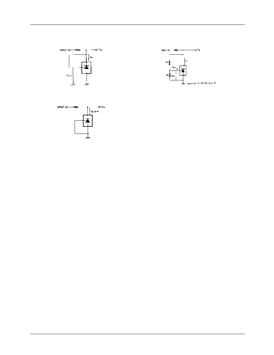
Test Circuits
Figure 1. Test Circuit for V
KA
=V
REF
Figure 2. Test Circuit for V
KA
V
REF
LM431S
LM431S
LM431S
Figure 3. Test Circuit for l
KA(OFF)
LM431SA/LM431SB/LM431SC
5
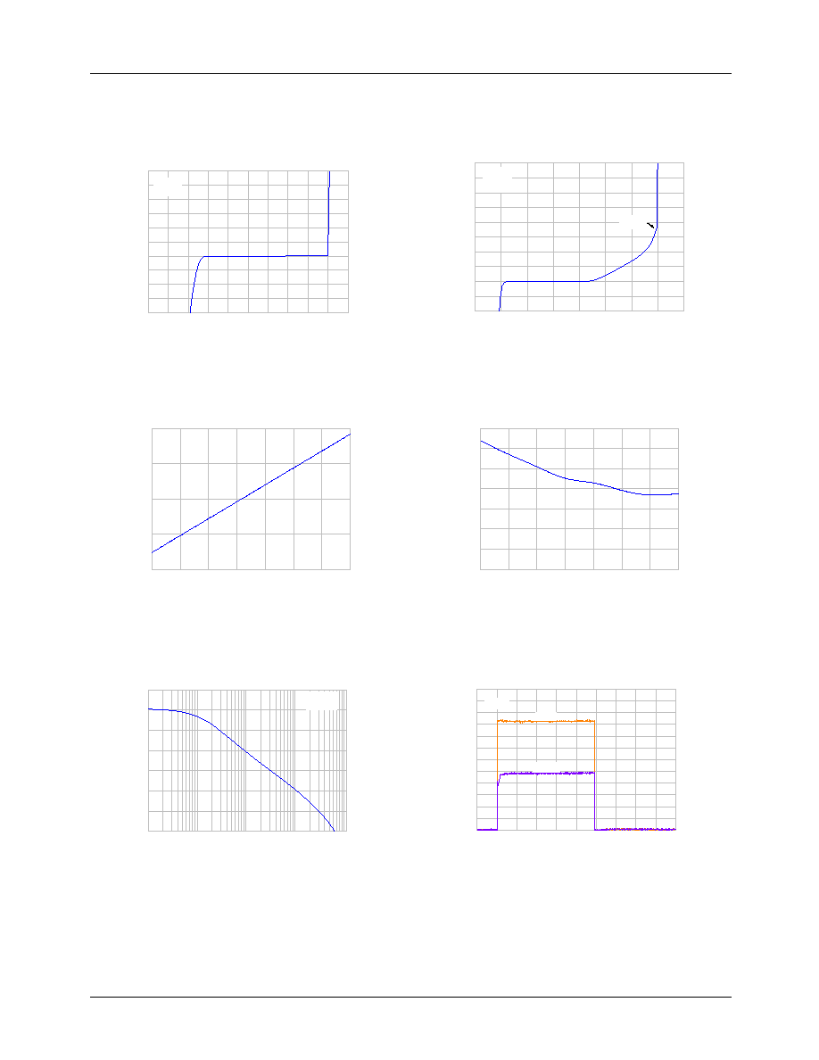
Typical Performance Characteristics
-2
-1
0
1
2
3
-100
-50
0
50
100
150
V
KA
= V
REF
T
A
= 25
o
C
I
K
,
C
a
th
o
d
e
C
u
r
r
e
n
t
(
m
A
)
V
KA
, Cathode Voltage (V)
-50
-25
0
25
50
75
100
125
0.000
0.025
0.050
0.075
0.100
I
of
f
,
O
ff-St
ate
C
a
th
od
e C
u
rren
t
(u
A)
T
A
, Ambient Temperature (
o
C)
1k
10k
100k
1M
10M
-10
0
10
20
30
40
50
60
T
A
= 25
o
C
I
KA
= 10mA
Op
en L
oop
Volt
a
ge G
a
in
(dB)
Frequency (Hz)
-1
0
1
2
3
-200
0
200
400
600
800
I
KA(MIN)
V
KA
= V
REF
T
A
= 25
o
C
I
KA
,
C
A
T
H
O
D
E
CURRE
NT
(
u
A
)
V
KA
, CATHODE VOLTAGE (V)
-50
-25
0
25
50
75
100
125
0.0
0.5
1.0
1.5
2.0
2.5
3.0
3.5
I
re
f
,
R
e
fe
ren
c
e Inp
u
t C
u
rre
nt (uA)
T
A
, Ambient Temperature (
o
C)
0
4
8
12
16
20
0
1
2
3
4
5
6
T
A
=25
o
C
OUTPUT
INPUT
Vo
lt
ag
e Sw
ing
(V)
Time (us)
Figure 4. Cathode Current vs. Cathode Voltage
Figure 5. Cathode Current vs. Cathode Voltage
Figure 6. OFF-State Cathode Current vs.
Ambient Temperature
Figure7. Reference Input Current vs.
Ambient Temperature
Figure 8. Small Signal Voltage Amplification vs. Frequency
Figure 9. Pulse Response
LM431SA/LM431SB/LM431SC
6
Typical Performance Characteristics
(Continued)
100p
1n
10n
100n
1µ
10µ
0
20
40
60
80
100
120
140
B
A
A V
KA
= Vref
B V
KA
= 5.0 V @ I
K
= 10
mA
T
A
= 25
o
C
I
K
,
CAT
H
ODE
CURRENT
(
m
A)
C
L
, LOAD CAPACITANCE
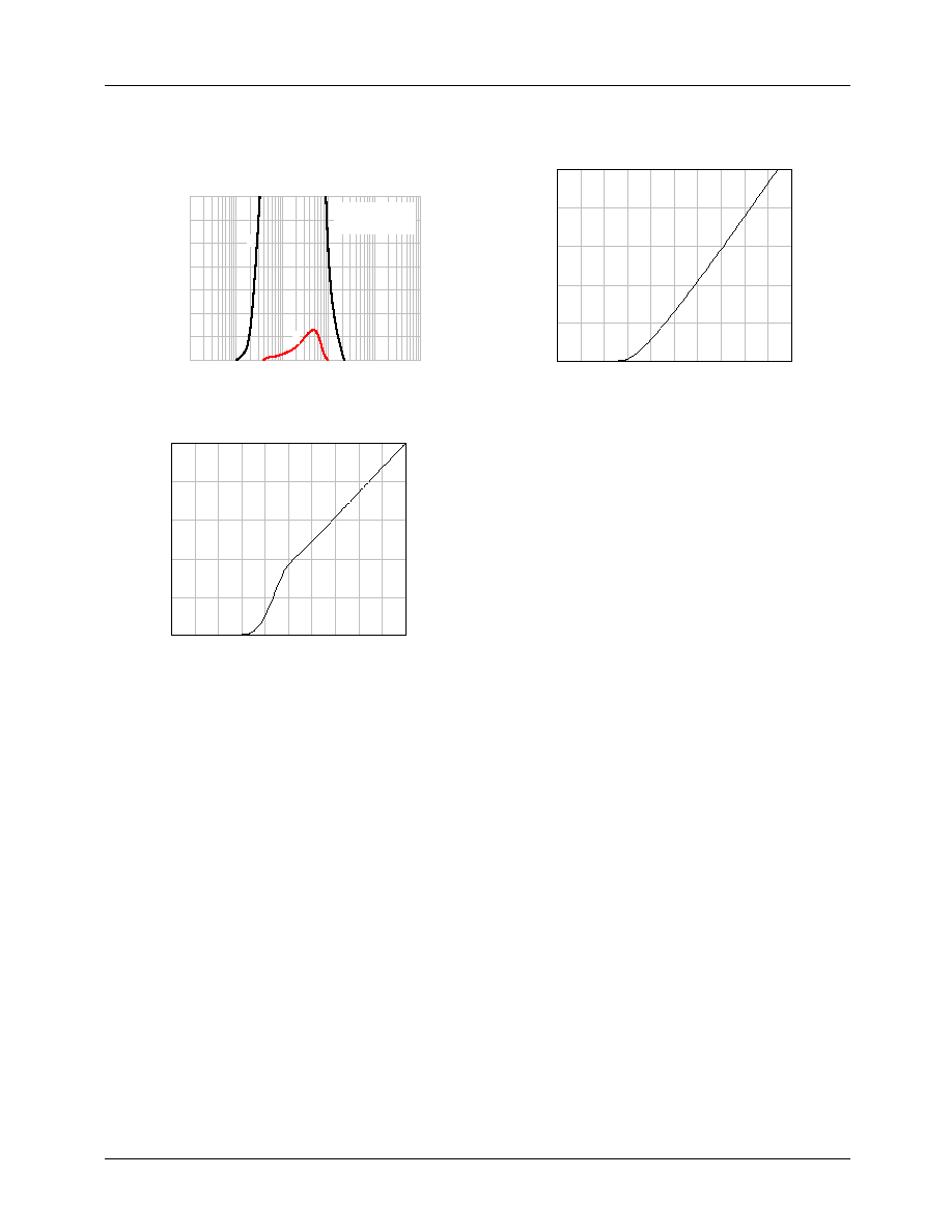
Figure 10. Stability Boundary Conditions
Figure 11. Anode-Reference Diode Curve
Figure 12. Reference-Cathode Diode Curve
0.0
0.2
0.4
0.6
0.8
1.0
1.2
1.4
1.6
1.8
2.0
0
1
2
3
4
5
Cur
r
en
t
(
m
A
)
Anode-Ref. Voltage(V)
0.0
0.2
0.4
0.6
0.8
1.0
1.2
1.4
1.6
1.8
2.0
0
1
2
3
4
5
Cur
r
en
t
(
m
A
)
Ref.-Cathode Voltage(V)
LM431SA/LM431SB/LM431SC
7
Typical Application
V
O
1
R
1
R
2
-------
+
V
ref
=
LM431S
V
O
V
ref
1
R
1
R
2
-------
+
=
LM431S
LM7805/MC7805
V
O
1
R
1
R
2
-------
+
V
ref
=
LM431S
LM431S
LM431S
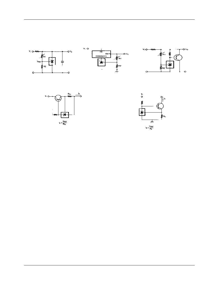
Figure 13
.
Shunt Regulator
Figure 14
.
Output Control for
-
Three-Termianl Fixed Regulator Figure 15. High Current Shunt Regulator
Figure 16. Current Limit or Current Source
Figure 17. Constant-Current Sink
LM431SA/LM431SB/LM431SC
8
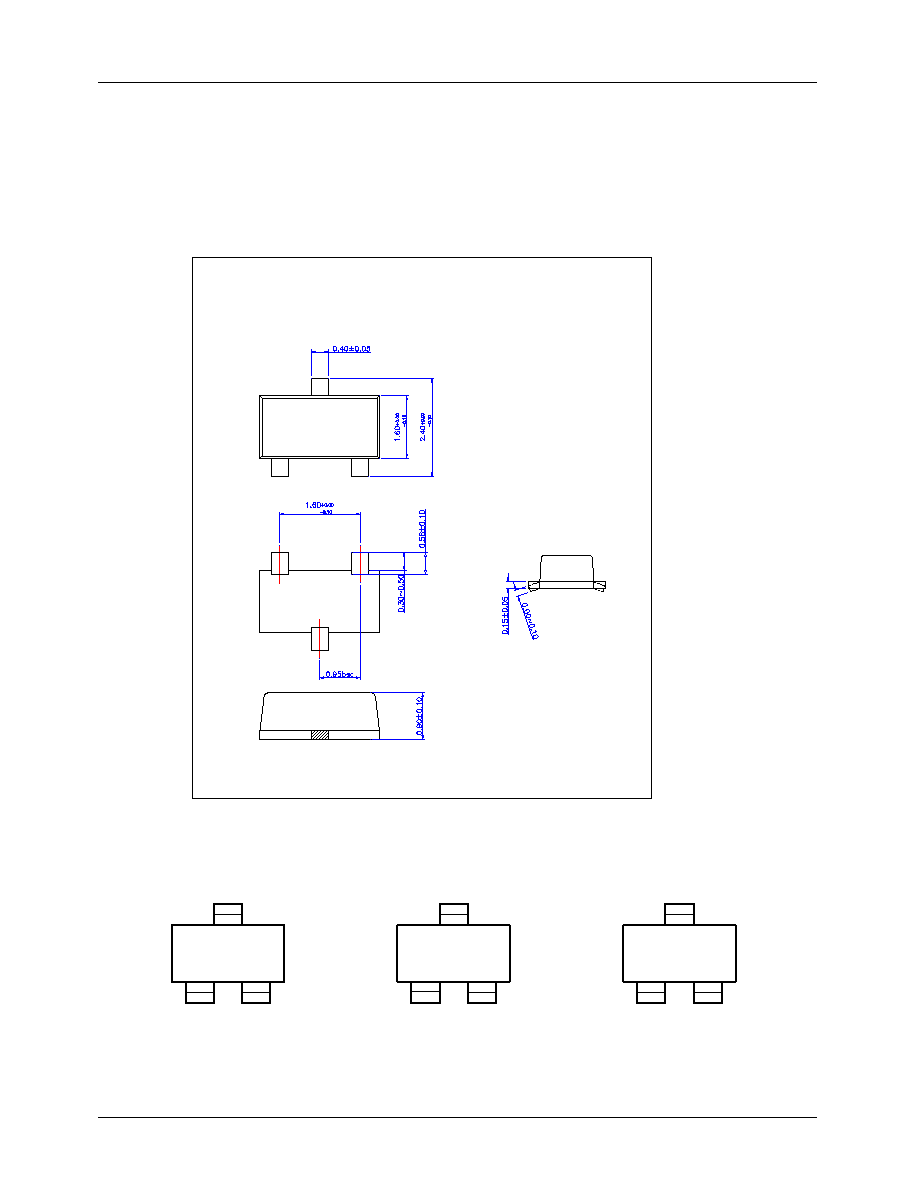
Mechanical Dimensions
Package
Dimensions in millimeters
Marking
SOT-23F
43A
43B
43C
2% tolerance
1% tolerance
0.5% tolerance
LM431SA/LM431SB/LM431SC
9
Mechanical Dimensions
(Continued)
Package
Dimensions in millimeters
Marking
SOT-89
0.40
±
0.10
2.50
±
0.20
(0.50)
(0.40)
4.10
±
0.20
0.40
+0.10
≠0.05
0.50
±
0.10
1.65
±
0.10
4.50
±
0.20
1.50
±
0.20
C0.2
1.50 TYP 1.50 TYP
(1.10)
43A
2% tolerance
1% tolerance
0.5% tolerance
43B
43C

LM431SA/LM431SB/LM431SC
11/14/02 0.0m 001
Stock#DSxxxxxxxx
2002 Fairchild Semiconductor Corporation
LIFE SUPPORT POLICY
FAIRCHILD'S PRODUCTS ARE NOT AUTHORIZED FOR USE AS CRITICAL COMPONENTS IN LIFE SUPPORT DEVICES
OR SYSTEMS WITHOUT THE EXPRESS WRITTEN APPROVAL OF THE PRESIDENT OF FAIRCHILD SEMICONDUCTOR
CORPORATION. As used herein:
1. Life support devices or systems are devices or systems
which, (a) are intended for surgical implant into the body,
or (b) support or sustain life, and (c) whose failure to
perform when properly used in accordance with
instructions for use provided in the labeling, can be
reasonably expected to result in a significant injury of the
user.
2. A critical component in any component of a life support
device or system whose failure to perform can be
reasonably expected to cause the failure of the life support
device or system, or to affect its safety or effectiveness.
www.fairchildsemi.com
DISCLAIMER
FAIRCHILD SEMICONDUCTOR RESERVES THE RIGHT TO MAKE CHANGES WITHOUT FURTHER NOTICE TO ANY
PRODUCTS HEREIN TO IMPROVE RELIABILITY, FUNCTION OR DESIGN. FAIRCHILD DOES NOT ASSUME ANY
LIABILITY ARISING OUT OF THE APPLICATION OR USE OF ANY PRODUCT OR CIRCUIT DESCRIBED HEREIN; NEITHER
DOES IT CONVEY ANY LICENSE UNDER ITS PATENT RIGHTS, NOR THE RIGHTS OF OTHERS.
Ordering Information
Product Number
Output Voltage Tolerance
Package
Operating Temperature
LM431SCCML
0.5%
SOT-89
-25 ~ +85
∞
C
LM431SCCMF
SOT-23F
LM431SBCML
1%
SOT-89
LM431SBCMF
SOT-23F
LM431SACML
2%
SOT-89
LM431SACMF SOT-23F