©2002 Fairchild Semiconductor Corporation
www.fairchildsemi.com
Rev. 1.0.4
Features
∑ Maximum Output Current of 100mA
∑ Output Voltage of 5V, 8V, 12V, 15V, 18V and 24V
∑ Thermal Overload Protection
∑ Short Circuit Current Limiting
∑ Output Voltage Offered in ±5% Tolerance
Description
The MC78LXXA/LM78LXXA/MC78L05AA series of
fixed voltage monolithic integrated circuit voltage
regulators are suitable for application that required supply
current up to 100mA.
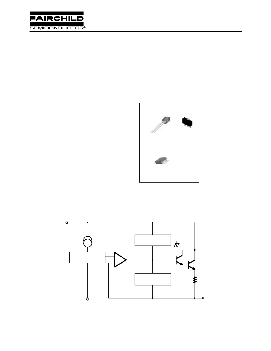
TO-92
1. Output 2. GND 3. Input
8-SOP
1. Output 2. GND 3. GND 4. NC
5. NC 6. GND 7. GND 8. Input
1
1
SOT-89
1
GND
2 3
2 3
8
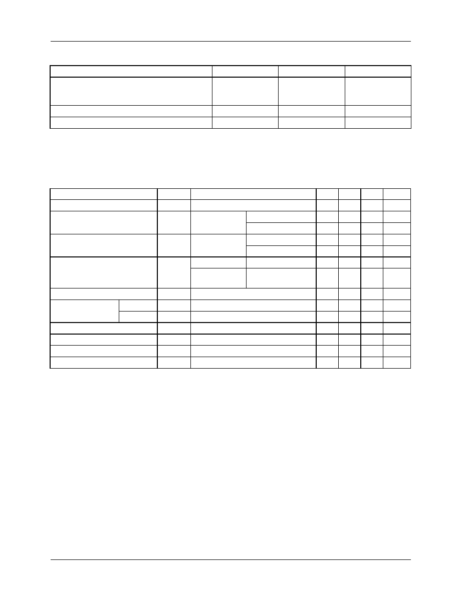
Internal Block Diagram
V
I
3
2
GND
V
0
1
I
R
SC
REFERENCE VOLTAGE
SHORT CIRCUIT
PROTECTION
THERMAL SHUTDOWN
CIRCUIT
+
-
Inpu
t
Outpu
t
MC78LXXA/LM78LXXA/MC78L05AA
3-Terminal 0.1A Positive Voltage Regulator
MC78LXXA/LM78LXXA/MC78L05AA
2
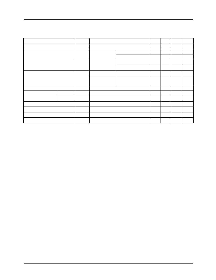
Absolute Maximum Ratings
Electrical Characteristics(MC78L05A/LM78L05A)
(V
I
= 10V, I
O
= 40mA, 0
∞
C
T
J
125
∞
C, C
I
= 0.33
µ
F, C
O
= 0.
1
µ
F, unless otherwise specified. (Note 1)
Note:
1. The maximum steady state usable output current and input voltage are very dependent on the heat sinking and/or lead length
of the package. The data above represent pulse test conditions with junction temperature as indicated at the initiation of tests.
2. Power dissipation P
D
0.75W.
Parameter
Symbol
Value
Unit
Input Voltage (for V
O
= 5V, 8V)
(for V
O
= 12V to 18V)
(for V
O
=
24V)
V
I
30
35
40
V
V
V
Operating Junction Temperature Range
T
J
0 ~ +150
∞
C
Storage Temperature Range
T
STG
-65 ~ +150
∞
C
Parameter
Symbol
Conditions
Min.
Typ. Max.
Unit
Output Voltage
V
O
T
J
= 25
∞
C
4.8
5.0
5.2
V
Line Regulation (Note1)
V
O
T
J
= 25
∞
C
7V
V
I
20V
-
8
150
mV
8V
V
I
20V
-
6
100
mV
Load Regulation (Note1)
V
O
T
J
= 25
∞
C
1mA
I
O
100mA
-
11
60
mV
1mA
I
O
40mA
-
5.0
30
mV
Output Voltage
V
O
7V
V
I
20V
1mA
I
O
40mA
-
-
5.25
V
7V
V
I
V
MAX
(Note 2)
1mA
I
O
70mA
4.75
-
5.25
V
Quiescent Current
I
Q
T
J
= 25
∞
C
-
2.0
5.5
mA
Quiescent Current
Change
With Line
I
Q
8V
V
I
20V
-
-
1.5
mA
With Load
I
Q
1mA
I
O
40
mA
-
-
0.1
mA
Output Noise Voltage
V
N
T
A
= 25
∞
C, 10Hz
f
100kHz
-
40
-
µ
V/Vo
Temperature Coefficient of V
O
V
O
/
T
I
O
= 5mA
-
-0.65
-
mV/
∞
C
Ripple Rejection
RR
f = 120Hz, 8V
V
I
18V, T
J
= 25
∞
C
41
80
-
dB
Dropout Voltage
V
D
T
J
= 25
∞
C
-
1.7
-
V
MC78LXXA/LM78LXXA/MC78L05AA
3
Electrical Characteristics(MC78L08A)
(Continued)
(V
I
= 14V, I
O
= 40mA, 0
∞
C
T
J
125
∞
C, C
I
= 0.33
µ
F, C
O
= 0.
1
µ
F, unless otherwise specified. (Note 1)
Note:
1. The maximum steady state usable output current and input voltage are very dependent on the heat sinking and/or lead length
of the package. The data above represent pulse test conditions with junction temperature as indicated at the initiation of tests.
2. Power dissipation P
D
0.75W.
Parameter
Symbol
Conditions
Min. Typ. Max.
Unit
Output Voltage
V
O
T
J
= 25
∞
C
7.7
8.0
8.3
V
Line Regulation (Note1)
V
O
T
J
= 25
∞
C
10.5V
V
I
23V
-
10
175
mV
11V
V
I
23V
-
8
125
mV
Load Regulation (Note1)
V
O
T
J
= 25
∞
C
1mA
I
O
100mA
-
15
80
mV
1mA
I
O
40mA
-
8.0
40
mV
Output Voltage
V
O
10.5V
V
I
23V 1mA
I
O
40mA
7.6
-
8.4
V
10.5V
V
I
V
MAX
(Note 2)
1mA
I
O
70mA
7.6
-
8.4
V
Quiescent Current
I
Q
T
J
= 25
∞
C
-
2.0
5.5
mA
Quiescent Current
Change
With Line
I
Q
11V
V
I
23V
-
-
1.5
mA
With Load
I
Q
1mA
I
O
40mA
-
-
0.1
mA
Output Noise Voltage
V
N
T
A
= 25
∞
C, 10Hz
f
100kHz
-
60
-
µ
V/Vo
Temperature Coefficient of V
O
V
O
/
T
I
O
= 5mA
-
-0.8
-
mV/
∞
C
Ripple Rejection
RR
f = 120Hz, 11V
V
I
21V, T
J
= 25
∞
C
39
70
-
dB
Dropout Voltage
V
D
T
J
= 25
∞
C
-
1.7
-
V
MC78LXXA/LM78LXXA/MC78L05AA
4
Electrical Characteristics(MC78L12A/LM78L12A)
(Continued)
(V
I
= 19V, I
O
= 40mA, 0
∞
C
T
J
125
∞
C, C
I
= 0.33
µ
F, C
O
= 0.
1
µ
F, unless otherwise specified. (Note 1)
Note:
1. The maximum steady state usable output current and input voltage are very dependent on the heat sinking and/or lead length
of the package. The data above represent pulse test conditions with junction temperature as indicated at the initiation of tests.
2. Power dissipation P
D
0.75W.
Parameter
Symbol
Conditions
Min.
Typ. Max.
Unit
Output Voltage
V
O
T
J
= 25
∞
C
11.5
12
12.5
V
Line Regulation (Note1)
V
O
T
J
= 25
∞
C
14.5V
V
I
27V
-
20
250
mV
16V
V
I
27V
-
15
200
mV
Load Regulation (Note1)
V
O
T
J
= 25
∞
C
1mA
I
O
100mA
-
20
100
mV
1mA
I
O
40mA
-
10
50
mV
Output Voltage
V
O
14.5V
V
I
27V 1mA
I
O
40mA
11.4
-
12.6
V
14.5V
V
I
V
MAX
(Note 2)
1mA
I
O
70mA
11.4
-
12.6
V
Quiescent Current
I
Q
T
J
= 25
∞
C
-
2.1
6.0
mA
Quiescent Current
Change
With Line
I
Q
16V
V
I
27V
-
-
1.5
mA
With Load
I
Q
1mA
I
O
40mA
-
-
0.1
mA
Output Noise Voltage
V
N
T
A
= 25
∞
C, 10Hz
f
100kHz
-
80
-
µ
V/Vo
Temperature Coefficient of V
O
V
O
/
T
I
O
= 5mA
-
-1.0
-
mV/
∞
C
Ripple Rejection
RR
f = 120Hz, 15V
V
I
25V, T
J
= 25
∞
C
37
65
-
dB
Dropout Voltage
V
D
T
J
= 25
∞
C
-
1.7
-
V
MC78LXXA/LM78LXXA/MC78L05AA
5
Electrical Characteristics(MC78L15A)
(Continued)
(V
I
= 23V, I
O
= 40mA, 0
∞
C
T
J
125
∞
C, C
I
= 0.33
µ
F, C
O
= 0.
1
µ
F, unless otherwise specified. (Note 1)
Note:
1. The maximum steady state usable output current and input voltage are very dependent on the heat sinking and/or lead length
of the package. The data above represent pulse test conditions with junction temperature as indicated at the initiation of tests.
2. Power dissipation P
D
0.75W.
Parameter
Symbol
Conditions
Min.
Typ. Max.
Unit
Output Voltage
V
O
T
J
= 25
∞
C
14.4
15
15.6
V
Line Regulation (Note1)
V
O
T
J
= 25
∞
C
17.5V
V
I
30V
-
25
300
mV
20V
V
I
30V
-
20
250
mV
Load Regulation (Note1)
V
O
T
J
= 25
∞
C
1mA
I
O
100mA
-
25
150
mV
1mA
I
O
40mA
-
12
75
mV
Output Voltage
V
O
17.5V
V
I
30V 1mA
I
O
40mA
14.25
-
15.75
V
17.5V
V
I
V
MAX
(Note 2)
1mA
I
O
70mA
14.25
-
15.75
V
Quiescent Current
I
Q
T
J
= 25
∞
C
-
2.1
6.0
mA
Quiescent Current
Change
With Line
I
Q
20V
V
I
30V
-
-
1.5
mA
With Load
I
Q
1mA
I
O
40mA
-
-
0.1
mA
Output Noise Voltage
V
N
T
A
= 25
∞
C, 10Hz
f
100kHz
-
90
-
µ
V/Vo
Temperature Coefficient of V
O
V
O
/
T I
O
= 5mA
-
-1.3
-
mV/
∞
C
Ripple Rejection
RR
f = 120Hz, 18.5V
V
I
28.5V, T
J
= 25
∞
C
34
60
-
dB
Dropout Voltage
V
D
T
J
= 25
∞
C
-
1.7
-
V