 | –≠–ª–µ–∫—Ç—Ä–æ–Ω–Ω—ã–π –∫–æ–º–ø–æ–Ω–µ–Ω—Ç: MC7912A | –°–∫–∞—á–∞—Ç—å:  PDF PDF  ZIP ZIP |
©2002 Fairchild Semiconductor Corporation
www.fairchildsemi.com
Rev. 1.0.1
Features
∑ Output Current in Excess of 1A
∑ Output Voltages of -5, -6, -8 , -9, -10, -12, -15, -18 and -
24V
∑ Internal Thermal Overload Protection
∑ Short Circuit Protection
∑ Output Transistor Safe Operating Area Compensation
Description
The MC79XX / MC79XXA/ LM79XX series of three
terminal negative regulators are available in TO-220
package and with several fixed output voltages, making
them useful in a wide range of applications. Each type
employs internal current limiting, thermal shut down and
safe operating area protection, making it essentially
indestructible.
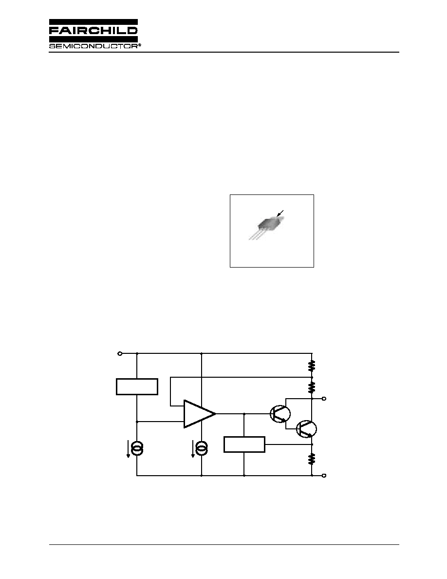
TO-220
1. GND 2. Input 3. Output
1
Vin
Internal Block Digram
VOLTAGE
REFERENCE
+
-
PROTECTION
CIRCUITRY
R1
R2
Rsc
GND
I1
I2
Out
In
Q1
Q2
Output
Input
MC79XX/MC79XXA/LM79XX
3-Terminal 1A Negative Voltage Regulator

MC79XX/MC79XXA/LM79XX
2
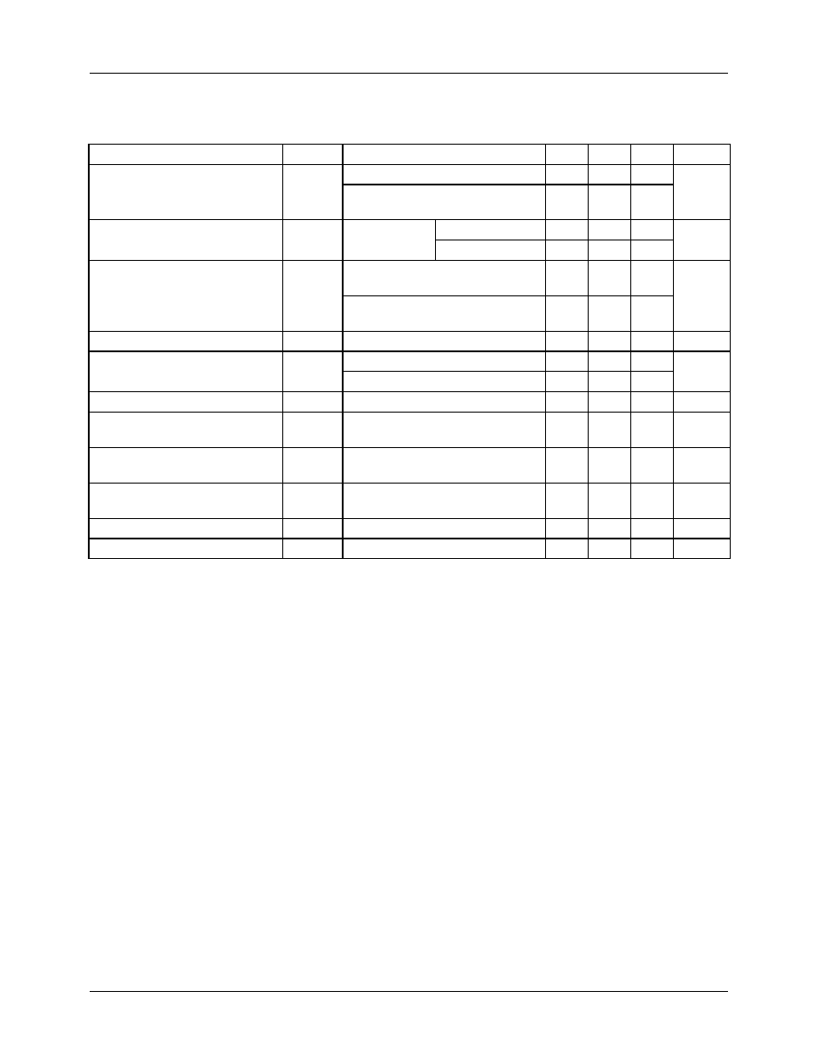
Absolute Maximum Ratings
Note:
1. Thermal resistance test board
Size: 76.2mm * 114.3mm * 1.6mm(1S0P)
JEDEC standard: JESD51-3, JESD51-7
2. Assume no ambient airflow
Electrical Characteristics (MC7905/LM7905)
(V
I
= -10V, I
O
= 500mA, 0
∞
C
T
J
+125
∞
C, C
I
=2.2
µ
F, C
O
=1
µ
F, unless otherwise specified.)
Note
3. Load and line regulation are specified at constant junction temperature. Changes in V
O
due to heating effects must be taken
into account separately. Pulse testing with low duty is used.
Parameter
Symbol
Value
Unit
Input Voltage
V
I
-35
V
Thermal Resistance Junction-Case (Note1)
R
JC
5
∞
C/W
Thermal Resistance Junction-Air (Note1, 2)
R
JA
65
Operating Temperature Range
T
OPR
0 ~ +125
∞
C
Storage Temperature Range
T
STG
-65 ~ +150
∞
C
Parameter
Symbol
Conditions
Min.
Typ.
Max.
Unit
Output Voltage
V
O
T
J
= +25
∞
C
-4.8
-5.0
-5.2
V
I
O
= 5mA to 1A, P
O
15W
V
I
= -7V to -20V
-4.75
-5.0
-5.25
Line Regulation (Note3)
V
O
T
J
= +25
∞
C
V
I
= -7V to -25V
-
35
100
mV
V
I
= -8V to -12V
-
8
50
Load Regulation (Note3)
V
O
T
J
= +25
∞
C
I
O
= 5mA to 1.5A
-
10
100
mV
T
J
=+25
∞
C
I
O
= 250mA to 750mA
-
3
50
Quiescent Current
I
Q
T
J
=+25
∞
C
-
3
6
mA
Quiescent Current Change
I
Q
I
O
= 5mA to 1A
-
0.05
0.5
mA
V
I
= -8V to -25V
-
0.1
0.8
Temperature Coefficient of V
D
Vo/
T
I
O
= 5mA
-
- 0.4
-
mV/
∞
C
Output Noise Voltage
V
N
f = 10Hz to 100kHz
T
A
=+25
∞
C
-
40
-
µ
V
Ripple Rejection
RR
f = 120Hz
V
I
= 10V
54
60
-
dB
Dropout Voltage
V
D
T
J
= +25
∞
C
I
O
= 1A
-
2
-
V
Short Circuit Current
I
SC
T
J
=+25
∞
C, V
I
= -35V
-
300
-
mA
Peak Current
I
PK
T
J
=+25
∞
C
-
2.2
-
A

MC79XX/MC79XXA/LM79XX
3
Electrical Characteristics (MC7906)
(Continued)
(V
I
= -11V, I
O
= 500mA, 0
∞
C
T
J
+125
∞
C, C
I
=2.2
µ
F, C
O
=1
µ
F, unless otherwise specified.)
Note
1. Load and line regulation are specified at constant junction temperature. Changes in V
O
due to heating effects must be taken
into account separately. Pulse testing with low duty is used.
Parameter
Symbol
Conditions
Min.
Typ.
Max.
Unit
Output Voltage
V
O
T
J
= +25
∞
C
-5.75
-6
-6.25
V
I
O
= 5mA to 1A, P
O
15W
V
I
= -9V to -21V
-5.7
-6
-6.3
Line Regulation (Note1)
V
O
T
J
= +25
∞
C
V
I
= -8V to -25V
-
10
120
mV
V
I
= -9V to -13V
-
5
60
Load Regulation (Note1)
V
O
T
J
= +25
∞
C
I
O
= 5mA to 1.5A
-
10
120
mV
T
J
=+25
∞
C
I
O
= 250mA to 750mA
-
3
60
Quiescent Current
I
Q
T
J
=+25
∞
C
-
3
6
mA
Quiescent Current Change
I
Q
I
O
= 5mA to 1A
-
0.05
0.5
mA
V
I
= -8V to -25V
-
0.1
1.3
Temperature Coefficient of V
D
Vo/
T
I
O
= 5mA
-
-0.5
-
mV/
∞
C
Output Noise Voltage
V
N
f = 10Hz to 100kHz
T
A
=+25
∞
C
-
130
-
µ
V
Ripple Rejection
RR
f = 120Hz
V
I
= 10V
54
60
-
dB
Dropout Voltage
V
D
T
J
= +25
∞
C
I
O
= 1A
-
2
-
V
Short Circuit Current
I
SC
T
J
= +25
∞
C, V
I
= -35V
-
300
-
mA
Peak Current
I
PK
T
J
= +25
∞
C
-
2.2
-
A
MC79XX/MC79XXA/LM79XX
4
Electrical Characteristics (MC7908)
(Continued)
(V
I
= -14V, I
O
= 500mA, 0
∞
C
T
J
+125
∞
C, C
I
=2.2
µ
F, C
O
=1
µ
F, unless otherwise specified.)
Note
1. Load and line regulation are specified at constant junction temperature. Changes in V
O
due to heating effects must be taken
into account separately. Pulse testing with low duty is used.
Parameter
Symbol
Conditions
Min.
Typ.
Max.
Unit
Output Voltage
V
O
T
J
= +25
∞
C
-7.7
-8
-8.3
V
I
O
= 5mA to 1A, P
O
15W
V
I
= -10V to -23V
-7.6
-8
-8.4
Line Regulation (Note1)
V
O
T
J
= +25
∞
C
V
I
= -10.5V to -25V
-
10
160
mV
V
I
= -11V to -17V
-
5
80
Load Regulation (Note1)
V
O
T
J
= +25
∞
C
I
O
= 5mA to 1.5A
-
12
160
mV
T
J
=+25
∞
C
I
O
= 250mA to 750mA
-
4
80
Quiescent Current
I
Q
T
J
=+25
∞
C
-
3
6
mA
Quiescent Current Change
I
Q
I
O
= 5mA to 1A
-
0.05
0.5
mA
V
I
= -10.5V to -25V
-
0.1
1
Temperature Coefficient of V
D
Vo/
T
I
O
= 5mA
-
-0.6
-
mV/
∞
C
Output Noise Voltage
V
N
f = 10Hz to 100kHz
T
A
=+25
∞
C
-
175
-
µ
V
Ripple Rejection
RR
f = 120Hz
V
I
= 10V
54
60
-
dB
Dropout Voltage
V
D
T
J
= +25
∞
C
I
O
= 1A
-
2
-
V
Short Circuit Current
I
SC
T
J
= +25
∞
C, V
I
= -35V
-
300
-
mA
Peak Current
I
PK
T
J
= +25
∞
C
-
2.2
-
A

MC79XX/MC79XXA/LM79XX
5
Electrical Characteristics (MC7909)
(Continued)
(V
I
= -15V, I
O
= 500mA, 0
∞
C
T
J
+125
∞
C, C
I
=2.2
µ
F, C
O
=1
µ
F, unless otherwise specified.)
Note:
1. Load and line regulation are specified at constant junction temperature. Changes in V
O
due to heating effects must be taken
into account separately. Pulse testing with low duty is used.
Parameter
Symbol
Conditions
Min.
Typ. Max.
Unit
Output Voltage
V
O
T
J
= +25
∞
C
-8.7
-9.0
-9.3
V
I
O
= 5mA to 1A, P
O
15W
V
I
= -1.5V to -23V
-8.6
-9.0
-9.4
Line Regulation (Note1)
V
O
T
J
= +25
∞
C
V
I
= -11.5V to -26V
-
10
180
mV
V
I
= -12V to -18V
-
5
90
Load Regulation (Note1)
V
O
T
J
= +25
∞
C
I
O
= 5mA to 1.5A
-
12
180
mV
T
J
= +25
∞
C
I
O
= 250mA to 750mA
-
4
90
Quiescent Current
I
Q
T
J
= +25
∞
C
-
3
6
mA
Quiescent Current Change
I
Q
I
O
= 5mA to 1A
-
0.05
0.5
mA
V
I
= -11.5V to -26V
-
0.1
1
Temperature Coefficient of V
D
Vo/
T
I
O
= 5mA
-
-0.6
-
mV/
∞
C
Output Noise Voltage
V
N
f = 10Hz to 100kHz
T
A
= +25
∞
C
-
175
-
µ
V
Ripple Rejection
RR
f = 120Hz
V
I
= 10V
54
60
-
dB
Dropout Voltage
V
D
T
J
= +25
∞
C
I
O
= 1A
-
2
-
V
Short Circuit Current
I
SC
T
J
= +25
∞
C, V
I
= -35V
-
300
-
mA
Peak Current
I
PK
T
J
= +25
∞
C
-
2.2
-
A