 | ÐлекÑÑоннÑй компоненÑ: MID400 | СкаÑаÑÑ:  PDF PDF  ZIP ZIP |
Äîêóìåíòàöèÿ è îïèñàíèÿ www.docs.chipfind.ru
7/24/03
Page 1 of 11
© 2003 Fairchild Semiconductor Corporation
AC LINE MONITOR
LOGIC-OUT DEVICE
MID400
DESCRIPTION
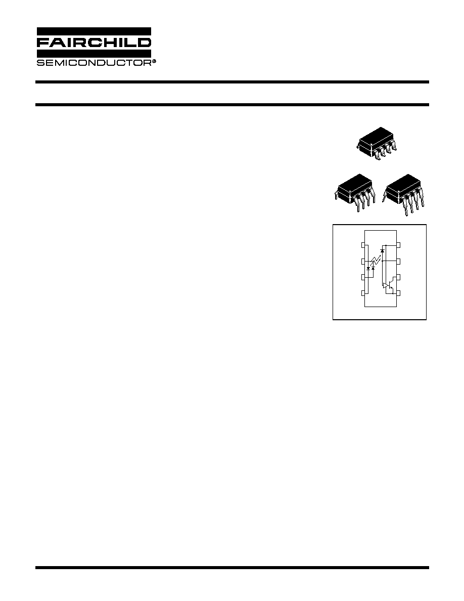
The MID400 is an optically isolated AC line-to-logic interface device. It is packaged
in an 8-lead plastic DIP. The AC line voltage is monitored by two back-to-back GaAs
LED diodes in series with an external resistor. A high gain detector circuit senses the
LED current and drives the output gate to a logic low condition.
The MID400 has been designed solely for the use as an
AC line monitor
. It is
recommended for use in any AC-to-DC control application where excellent optical
isolation, solid state reliability, TTL compatibility, small size, low power, and low
frequency operations are required.
FEATURES
·
Direct operation from any line voltage with the use of an external resistor.
·
Externally adjustable time delay
·
Externally adjustable AC voltage sensing level
·
High voltage isolation between input and output
·
Compact plastic DIP package
·
Logic level compatibility
·
UL recognized (File #E90700)
·
VDE recognized (file #102915),
add option V (e.g., MID400V)
APPLICATIONS
·
Monitoring of the AC/DC "line-down" condition
·
"Closed-loop" interface between electromechanical elements such
as solenoids, relay contacts, small motors, and microprocessors
·
Time delay isolation switch
1
2
3
4
5
6
7
8
V
CC
AUX
V
0
GND
Equivalent Circuit
N/C
N/C
8
8
1
8
1
1
AC LINE MONITOR
LOGIC-OUT DEVICE
MID400
7/24/03
Page 2 of 11
© 2003 Fairchild Semiconductor Corporation
ABSOLUTE MAXIMUM RATINGS
Rating
Value
Unit
EMITTER
RMS Current
25
mA
DC Current
±30
mA
LED Power Dissipation @ T
A
= 25°C (P
D
)
Derate above 70°C
45
2.0
mW
mW/°C
DETECTOR
Low Level Output Current (I
OL
)
20
mA
High Level Output Voltage(V
OH
)
7.0
V
Supply Voltage (V
CC
)
7.0
V
Detector Power Dissipation @ T
A
= 25°C (P
D
)
Derate above 70°C
70
2.0
mW
mW/°C
TOTAL DEVICE
Storage Temperature
-55 to +125
°C
Operating Temperature
-40 to +85
°C
Lead Solder Temperature
260 for 10 sec
°C
Total Device Power Dissipation @ T
A
= 25°C (P
D
)
Derate above 70°C
115
mW
4.0
mW/°C
Steady State Isolation
2500
VRMS
7/24/03
Page 3 of 11
© 2003 Fairchild Semiconductor Corporation
AC LINE MONITOR
LOGIC-OUT DEVICE
MID400
(RMS = True RMS Voltage at 60 Hz, THD
1%)
ELECTRICAL CHARACTERISTICS
(0°C to 70°C Free Air Temperature unless otherwise specified-All typical values are at 25°C
INDIVIDUAL COMPONENT CHARACTERISTICS
Parameter
Test Conditions
Symbol
Min
Typ
Max
Unit
EMITTER
Input Forward Voltage
(I
F
= ±30 mA, DC)
V
F
1.5
V
DETECTOR
Logic Low Output Supply Current
(I
IN
= 4.0 mA RMS,
V
O
= Open, V
CC
= 5.5 V,
24 V [ V
I (ON)
, RMS
240 V)
I
CCL
3.0
mA
Logic High Output
Supply Current
(I
IN
= 0.15 mA RMS, V
CC
= 5.5 V,
V
I (OFF)
, RMS
5.5 V)
I
CCH
0.80
mA
TRANSFER CHARACTERISTICS
DC Characteristics
Test Conditions
Symbol
Min
Typ
Max
Units
Logic Low
Output Current
(I
IN
= I
I (ON)
RMS, I
O
= 16 mA, V
CC
= 4.5 V,
24 V
V
I (ON)
, RMS
240 V)
V
OL
0.18
0.40
V
Logic High
Output Current
(I
IN
= 0.15 mA RMS, V
O
= V
CC
= 5.5 V,
V
I (OFF)
, RMS
5.5 V)
I
OH
0.02
100
µA
On-state RMS Input Voltage
(V
O
= 0.4 V, I
O
= 16 mA
V
CC
= 4.5 V, R
IN
= 22 K
)
V
I (ON)
RMS
90
V
Off-state RMS Input Voltage
(V
O
= V
CC
= 5.5 V,
I
O
100 µA, R
IN
= 22 K
)
V
I (OFF)
RMS
5.5
V
On-state RMS
Input Current
(V
O
= 0.4 V, I
O
= 16 mA, V
CC
= 4.5 V,
24 V
V
I (ON)
, RMS
240 V)
I
I (ON)
RMS
4.0
mA
Off-state RMS Input Current
(V
O
= V
CC
= 5.5 V, I
O
100 µA,
V
I (OFF)
, RMS
5.5 V)
I
I (OFF)
RMS
0.15
mA
TRANSFER CHARACTERISTICS
Characteristics
Test Conditions
Symbol
Min
Typ
Max
Units
SWITCHING TIME
(T
A
= 25°C)
Turn-On Time
(I
IN
= 4.0 mA RMS,
I
O
= 16 mA, V
CC
= 4.5 V,
R
IN
= 22 K
) (See Test Circuit 2)
t
ON
1.0
ms
Turn-Off Time
(I
IN
= 4.0 mA RMS,
I
O
= 16 mA, V
CC
= 4.5 V,
R
IN
= 22 K
) (See Test Circuit 2)
t
OFF
1.0
ms
AC LINE MONITOR
LOGIC-OUT DEVICE
MID400
7/24/03
Page 4 of 11
© 2003 Fairchild Semiconductor Corporation
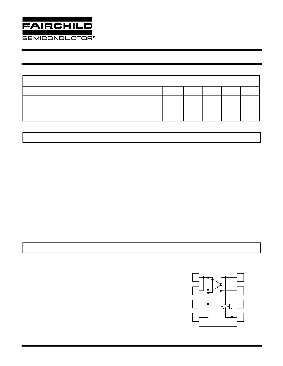
The input of the MID400 consists of two back-to-back LED diodes which will accept and convert alternating currents into light
energy. An integrated photo diode-detector amplifier forms the output network. Optical coupling between input and output provides
2500 VRMS voltage isolation. A very high current transfer ratio (defined as the ratio of the DC output current and the DC input cur-
rent) is achieved through the use of high gain amplifier. The detector amplifier circuitry operates from a 5 V DC supply and drives
an open collector transistor output. The switching times are intentionally designed to be slow in order to enable the MID400, when
used as an AC line monitor, to respond only to changes in input voltage exceeding many milliseconds. The short period of time
during zero-crossing which occurs once every half cycle of the power line is completely ignored. To operate the MID400, always
add a resistor, R
IN
, in series with the input (as shown in test circuit 1) to limit the current to the required value. The value of the
resistor can be determined by the following equation:
Where V
IN
(RMS) is the input voltage.
V
F
is the forward voltage drop across the LED.
I
IN
(RMS) is the desired input current required to sustain a logic "O" on the output.
DESIGNATION
PIN #
FUNCTION
V
IN1
, V
IN2
1,3
Input terminals
V
CC
8
Supply voltage, output circuit.
AUX.
7
Auxiliary terminal.
Programmable capacitor input to
adjust AC voltage sensing level and
time delay.
V
O
6
Output terminal; open collector.
GND
5
Circuit ground potential.
ISOLATION CHARACTERISTICS
(T
A
= 25°C)
Characteristics
Test Conditions
Symbol
Min
Typ
Max
Units
Steady State Isolation Voltage
Relative Humidity
50%, I
I-O
10 µA,
1 Minute, 60 Hz
V
ISO
2500
VRMS
Isolation Resistance
(V
I-O
= 500 VDC)
R
ISO
10
11
Isolation Capacitance
(f = 1 MHz)
C
ISO
2
pF
DESCRIPTION / APPLICATIONS
PIN DESCRIPTION
R
IN
V
IN
V
F
I
IN
-----------------------
=
4
5
1
V
IN1
V
IN2
V
CC
AUX.
GND
V
O
2
3
8
7
6
NOTE: DO NOT CONNECT PINS 2 AND 4
SCHEMATIC DIAGRAM

7/24/03
Page 5 of 11
© 2003 Fairchild Semiconductor Corporation
AC LINE MONITOR
LOGIC-OUT DEVICE
MID400
VOLTAGES
V
I (ON)
RMS
On-state RMS input voltage
The RMS voltage at an input terminal for a specified input current with output conditions applied that according
to the product specification will cause the output switching element to be sustained in the on-state within one
full cycle.
V
I (OFF)
RMS
Off-state RMS input voltage
The RMS voltage at an input terminal for a specified input current with output conditions applied that according
to the product specification will cause the output switching element to be sustained in the off-state within one
full cycle.
V
OL
Low-level output voltage
The voltage at an output terminal for a specific output current I
OL
, with input conditions applied that according
to the product specification will establish a low-level at the output.
V
OH
High-level output voltage
The voltage at an output terminal for a specific output current I
OH
, with input conditions applied that according
to the product specification will establish a high-level at the output.
V
F
LED forward voltage
The voltage developed across the LED when input current I
F
is applied to the anode of the LED.
CURRENTS
I
I (ON)
RMS
On-state RMS input current
The RMS current flowing into an input with output conditions applied that according to the product specification
will cause the output switching element to be sustained in the on-state within one full cycle.
I
I (OFF)
RMS
Off-state RMS input current
The RMS current flowing into an input with output conditions applied that according to the product specification
will cause the output switching element to be sustained in the off-state within one full cycle.
I
OH
High-level output current
The current flowing into * an output with input conditions applied that according to the product specification will
establish a high-level at the output.
I
OL
Low-level output current
The current flowing into * an output with input conditions applied that according to the product specification will
establish a low-level at the output.
I
CCL
Supply current, output low
The current flowing into * the V
CC
supply terminal of a circuit when the output is at a low-level voltage.
I
CCH
Supply current, output high
The current flowing into * the V
CC
supply terminal of a circuit when the output is at a high-level voltage.
DYNAMIC CHARACTERISTICS
t
ON
Turn-on time
The time between the specified reference points on the input and the output voltage waveforms with the output
changing from the defined high-level to the defined low-level.
t
OFF
Turn-off time
The time between the specified reference points on the input and the output voltage waveforms with the output
changing from the defined low-level to the defined high-level.
* Current flowing out of a terminal is a negative value.
GLOSSARY