 | ÐлекÑÑоннÑй компоненÑ: ML2021 | СкаÑаÑÑ:  PDF PDF  ZIP ZIP |
Äîêóìåíòàöèÿ è îïèñàíèÿ www.docs.chipfind.ru
www.fairchildsemi.com
REV. 1.1.1 3/19/01
Features
· Slope, height, and bandwidth adjustable
· Optimized group delays (500 Hz to 6.4 kHz)
· On chip anti-alias filter
· Bypass mode
· Low supply current 6 mA typical from ±5V supplies
· TTL / CMOS compatible interface
· Double buffered data latch
· Selectable master clock 1.544 or 1.536 MHz
· Synchronous or asynchronous data loading capability
· Compatible with ML2003 and ML2004 logarithmic
gain/attenuator
General Description
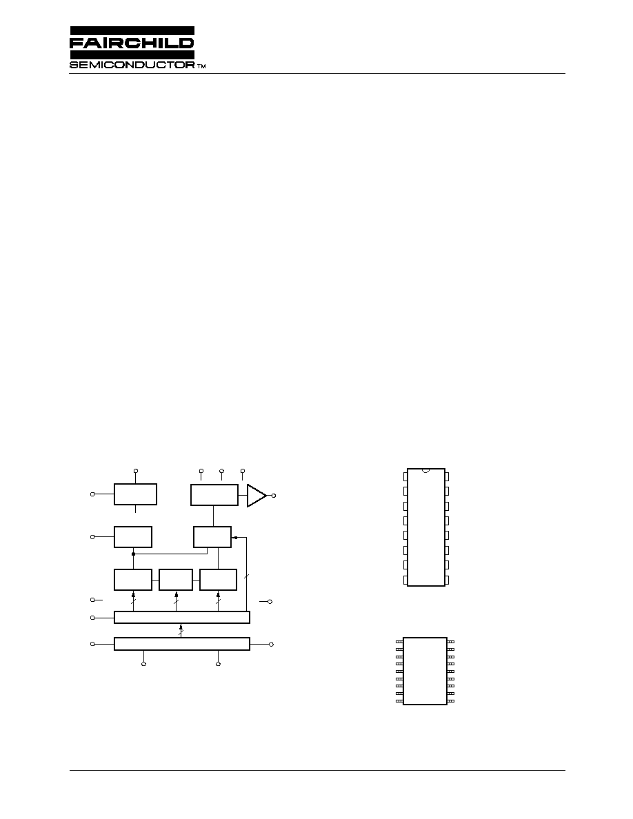
The ML2021 is a monolithic analog line equalizer for tele-
phone applications. The ML2021 consists of a switched
capacitor filter that realizes a family of frequency response
curves optimized for telephone line equalization while mini-
mizing group delay.
The ML2021 consists of a continuous anti-aliasing filter,
three programmable switched capacitor equalization filters,
an output smoothing filter, a 600
driver, and a digital
section for the serial interface.
The equalization filters adjust the slope, height, and band-
width of the frequency response. The desired frequency
response is programmed by a digital 14-bit serial input data
stream.
Block Diagram
Pin Connections
CLKSEL
AGND
CLKSEL
SID
NC
LATO
SCK
NC
SOD
CLK
CLKSEL
SID
NC
LATO
SCK
NC
SOD
CLK
V
CC
V
CC
P
DN
P
DN
V
OUT
AGND
AGND
V
IN
V
SS
V
SS
V
IN
V
OUT
LATI
LATI
NC
NC
GND
GND
TOP VIEW
TOP VIEW
1
1
2
3
4
5
6
7
8
9
18
17
16
15
14
13
12
11
10
2
3
4
5
6
7
8
16
15
14
13
12
11
10
9
CLK
CLOCK
GENERATOR
SMOOTHING
FILTER
MUX
ANTIALIAS
LO PASS
SLOPE
SECTION
HEIGHT
SECTION
BANDPASS
SECTION
V
CC
V
IN
P
DN
LATI
SID
V
OUT
GND
SOD
SCK
LATO
1
5
4
4
14
14-BIT LATCH
14-BIT SHIFT REGISTER
V
SS
ML2021
16-PIN DIP
ML2021
18-PIN SOIC
ML2021
Telephone Line Equalizer
ML2021
PRODUCT SPECIFICATION
2
REV. 1.1.1 3/19/01
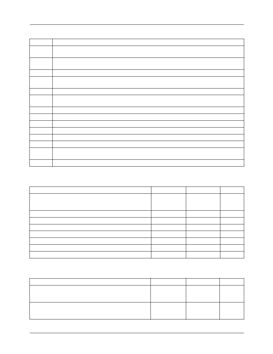
Pin Description
Absolute Maximum Ratings
1
Operating Conditions
Name
Function
CLKSEL
Clock select input.
This pin selects the frequency of the CLK input. If CLK is 1.536 MHz, set
CLKSEL = 1. If CLK is 1.544 MHz, set CLKSEL = 0. Pin has an internal pullup resistor to V
CC
.
SID
Serial input data.
Digital input that contains serial data word which controls the filter frequency
response setting.
LATO
Output latch clock.
Digital input which loads the data word back into the shift register from the latch.
SCK
Shift clock.
Digital input which shifts the serial data on SID into the shift register on rising edges and
out onto SOD on falling edges.
SOD
Serial output data.
Digital output of the shift register.
CLK
Master clock input.
Digital input which generates clocks for the switched capacitor filters.
Frequency can be either 1.544 MHz or 1.536 MHz.
GND
Digital ground.
0 volts. All digital inputs and output are referenced to this ground.
LATI
Input latch clock.
Digital input which loads data from the shift register into the latch.
V
SS
Negative supply.
5volts ±10%.
V
IN
Analog input.
AGND
Analog ground.
0 volts. Analog input and output are referenced to this ground.
V
OUT
Analog output.
P
DN
Powerdown input.
When P
DN
= 1, device is in powerdown mode. When P
ND
= 0, device is in normal
operation. This pin has an internal pulldown resistor to GND.
V
CC
Positive supply.
5 volts ± 10%
Parameter
Min.
Max. Units
Supply Voltage
V
CC
V
SS
+6.5
-6.5
V
V
AGND with respect to GND
±0.5
V
Analog Input and Output
V
SS
0.3
V
CC
+0.3
V
Digital Input and Outputs
GND 0.3
V
CC
+0.3
V
Input Current Per Pin
±25
mA
Power Dissipation
750
mW
Storage Temperature Range
-65
+150
°C
Lead Temperature (Soldering, 10 sec)
300
°C
Parameter
Min.
Max.
Units
Temperature Range
2
ML2021CX
ML2021IX
0
-40
70
85
°C
°C
Supply Voltage
V
CC
V
SS
4
-4
6
-6
V
V
PRODUCT SPECIFICATION
ML2021
REV. 1.1.1 3/19/01
3
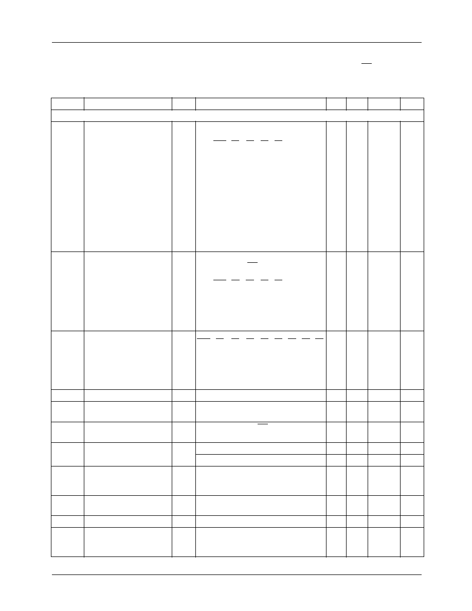
Electrical Characteristics
Unless otherwise specified T
A
= T
MIN
to T
MAX
, V
CC
= 5V ± 10%, V
SS
= -5V ± 10%, Data Word: BP = 1,
Other Bits = 0, C
L
= 100pF, R
L
= 600
, dBm measurements use 600
as reference load, V
IN
= -7dBm,
1kHz sinusoid CLK = 1.544 MHz ±300 Hz and digital time measured at 1.4 V
Symbol
Parameter
Notes
Conditions
Min Typ.
3
Max.
Units
Analog
SR
Response, Slope Section
4
1 kHz response
NL/L
S3
S2
S1
S0
0
0
0
0
0
1
1
1
1
1
1
0
0
0
1
1
0
0
0
0
1
1
0
0
1
0
1
0
0
0
1
0
1
0
1
0
0
1
0
0
1
0
0
1
1
0
0
0
1
0
1
0
0
0
1
1.4 ±0.1
2.6 ±0.2
4.7 ±0.2
7.8 ±0.2
11.4 ±0.25
0 ±0.1
0.4 ±0.1
0.9 ±0.2
1.8 ±0.2
3.7 ±0.2
6.6 ±0.25
dB
dB
dB
dB
dB
dB
dB
dB
dB
dB
dB
Referenced to
0
0
0
0
0
HR
Response, Height
Section
4
3250 Hz response referenced to 1 kHz
response with BP = 1, other bits = 0
NL/L
H3
H2
H1
H0
0
0
0
0
0
0
0
0
0
0
1
1
0
0
0
1
0
1
0
0
1
0
0
1
0
1
0
0
0
1
0 ±0.15
0.5 ±0.2
1.1 ±0.2
2.3 ±0.2
5.7 ±0.3
11.1 ±0.3
dB
dB
dB
dB
dB
dB
BR
Response, Bandwidth
Section (Q)
4
NL/L
B3
B2
B1
B0
H3
H2
H1
H0
0
0
0
0
0
0
0
0
0
0
1
1
0
0
0
1
0
1
0
0
1
0
0
1
0
1
0
0
0
1
1
1
1
1
1
1
1
1
1
1
1
1
1
1
1
1
1
1
1
1
1
1
1
1
16.1 ±2.0
14.2 ±1.5
12.6 ±1.5
9.1 ±1.0
3.6 ±0.5
1.2 ±0.35
PK
BW Peak Frequency
4
H3 thru H0 = 1
3230 3250
3270
Hz
AG
Absolute Gain, Flat
Response
4
0.5 kHz to 4 kHz
-0.1
+0.1
+0.3
dB
AGB
Absolute Gain, Bypass
Mode
4
0.3 kHz to 4 kHz, BP = 0
-0.1
+0.1
+0.3
dB
ICN
Idle Channel Noise
4
V
IN
= 0
3
8
dBrnc
V
IN
= 0, All Data Bits = 1
9
dBrnc
HD
Harmonic Distortion
4
V
IN
= 5 dBm, 1 kHz
Measure 2nd, 3rd, harmonic
relative to fundamental
-48
dB
SD
Signal to Distortion
4
V
IN
= -12dBm, 1 kHz
C msg weighted
+48
dB
SFN
Signal Frequency Noise
5
V
IN
= 0, 4 kHz
frequency
150 kHz
-50
dBm
PSRR
Power Supply Rejection
4
200mV
p-p
, 1 kHz sine, V
IN
= 0
on V
CC
on V
SS
-40
-40
dB
dB
ML2021
PRODUCT SPECIFICATION
4
REV. 1.1.1 3/19/01
Notes
1. Absolute maximum ratings are limits beyond which the life of the integrated circuit may be impaired. All voltages unless
otherwise specified are measured with respect to ground.
2. 0°C to +70°C and 40°C to +85°C operating temperature range devices are 100% tested with temperature limits guaranteed
by 100% testing, sampling, or by correlation with worst-case test conditions.
3. Typicals are parametric norm at 25°C.
4. Parameter guaranteed and 100% production tested.
5. Parameter guaranteed. Parameters not 100% tested are not in outgoing quality level calculation.
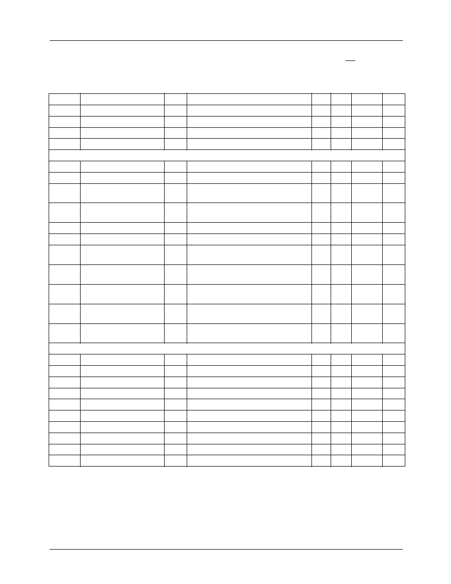
Z
IN
Input Impedance, V
IN
4
100
k
V
OS
Output Offset Voltage
4
V
IN
= 0
±50
mV
V
INR
Input Voltage Range
4
±2.0
V
V
OSW
Output Voltage Swing
4
R
L
= 600
±2.0
V
Digital and DC
V
IL
Digital Input Low Voltage
4
0.8
V
V
IH
Digital Input High Voltage
4
2.0
V
V
OL
Digital Output Low
Voltage
4
I
OL
= 2mA
0.4
V
V
OH
Digital Output High
Voltage
4
I
OH
= 1mA
4.0
V
I
LCLK
Input Current, CLK SEL
4
V
IN
= 0
5
100
µA
I
LPDN
Input Current, PDN
4
V
IN
= V
CC
-3
-100
µA
I
L
Input Current, All Other
Inputs
4
V
IN
= 0 to V
CC
±10
µA
I
CC
V
CC
Supply Current
4
No output load, V
IL
= GND,
V
IH
= V
CC
, V
IN
= 0
10
mA
I
SS
V
SS
Supply Current
4
No output load, V
IL
= GND,
V
IH
= V
CC
, V
IN
= 0
-10
mA
I
CCP
V
CC
Supply Current,
Powerdown Mode
4
No output load, V
IL
= GND,
V
IH
= V
CC
1.2
mA
I
SSP
V
SS
Supply Current,
Powerdown Mode
4
No output load, V
IL
= GND,
V
IH
= V
CC
-1.2
mA
AC Characteristics
t
DC
Clock Duty Cycle
5
40
60
%
t
SCK
SCK On/Off Period
4
250
ns
t
S
SID Data Setup Time
4
50
ns
t
H
SID Data Hold Time
4
50
ns
t
D
SOD Data Delay
4
0
125
ns
t
IPW
LATI Pulse Width
4
50
ns
t
OPW
LATO Pulse Width
4
50
ns
t
IS
, t
OS
LATI, LATO Setup Time
4
50
ns
t
IH
, t
OH
LATI, LATO Hold Time
5
50
ns
t
PLD
SOD Parallel Load Delay
4
0
125
ns
Electrical Characteristics
(continued)
Unless otherwise specified T
A
= T
MIN
to T
MAX
, V
CC
= 5V ± 10%, V
SS
= -5V ± 10%, Data Word: BP = 1,
Other Bits = 0, C
L
= 100pF, R
L
= 600
, dBm measurements use 600 as reference load, V
IN
= -7dBm,
1kHz sinusoid CLK = 1.544 MHz ±300 Hz and digital time measured at 1.4 V
Symbol
Parameter
Notes
Conditions
Min Typ.
3
Max.
Units
PRODUCT SPECIFICATION
ML2021
REV. 1.1.1 3/19/01
5
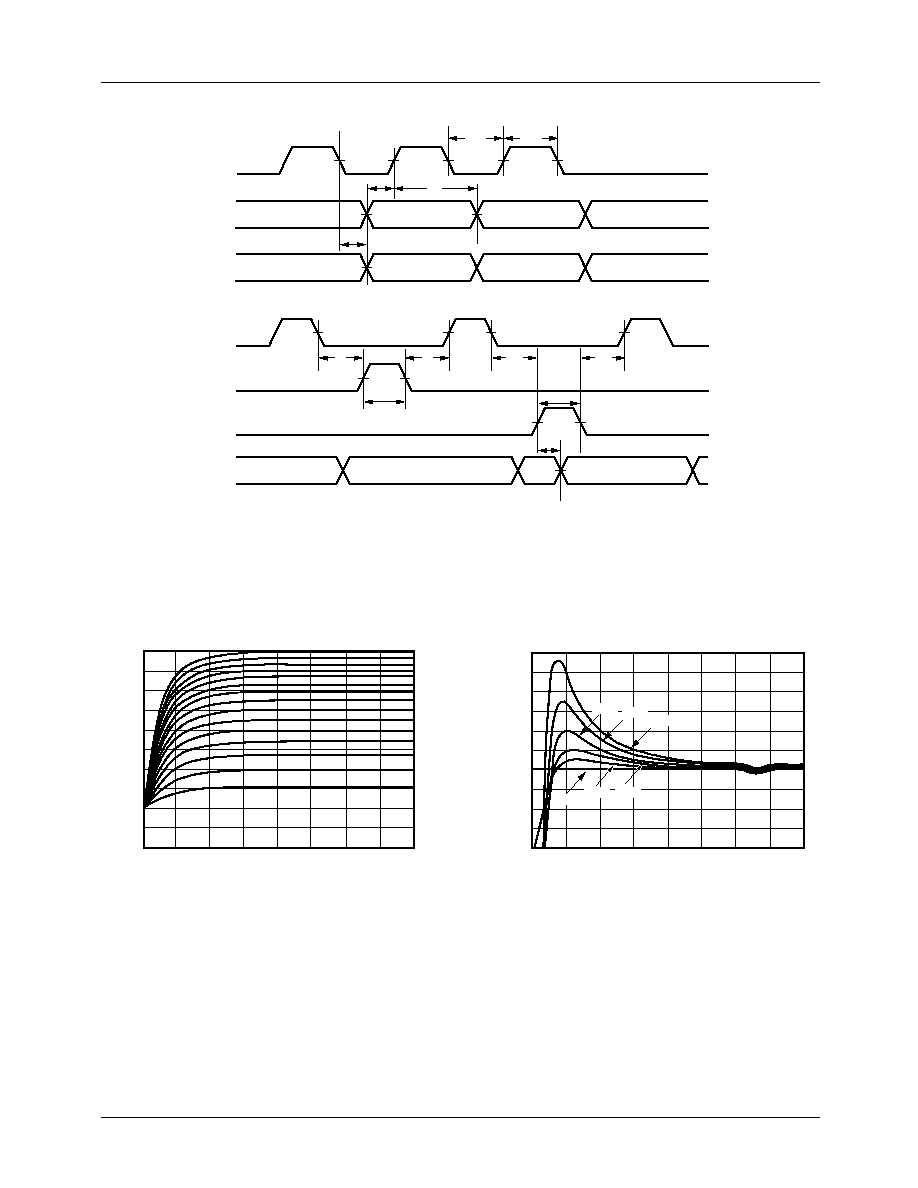
Figure 1. Serial Timing Diagram
Figure 2. Typical Slope Filter Response--NL/L = 0
B3-B0, H3-H0 = 0000, S3-S0 = 0000 to 1111.
SCK
t
SCK
t
SCK
t
S
t
IS
t
IH
t
OS
t
OH
t
IPW
t
OPW
t
PLD
t
D
t
H
SID
SOD
SCK
LATI
LATO
SOD
TIMING PARAMETERS ARE REFERENCED TO THE 1.4 VOLT MIDPOINT.
12
10.5
9.0
7.5
6.0
4.5
3.0
1.5
0
0
500
1000
1500
2000
FREQUENCY (Hz)
AMPLITUDE (dB)
2500
3000
3500
4000
0000
1111
1.5
3.0
0
500
1000
1500
2000
FREQUENCY (Hz)
2500
3000
3500
4000
100
120
80
60
40
20
0
20
40
GR
OUP DELA
Y
--
d
/df(
µ
s)
60
80
0100 1000
1111
0010
0001
0000