 | ÐлекÑÑоннÑй компоненÑ: ML2036C | СкаÑаÑÑ:  PDF PDF  ZIP ZIP |
ML2036 Serial Input Programmable Sine Wave Generator with Digital Gain Control
www.fairchildsemi.com
REV. 1.0.2 7/26/01
Features
· Programmable output frequency DC to 50kHz
· Low gain error and total harmonic distortion
· 3-wire SPI compatible serial microprocessor interface
with double buffered data latch
· Fully integrated solution no external components
required
· Frequency resolution of 1.5Hz (±0.75Hz) with a 12MHz
clock input
· Onboard 3 to 12MHz crystal oscillator
· Clock outputs of 1/2 or 1/8 of the input clock frequency
· Synchronous or asynchronous data loading capability
· Compatible with ML2004 logarithmic gain/attenuator
General Description
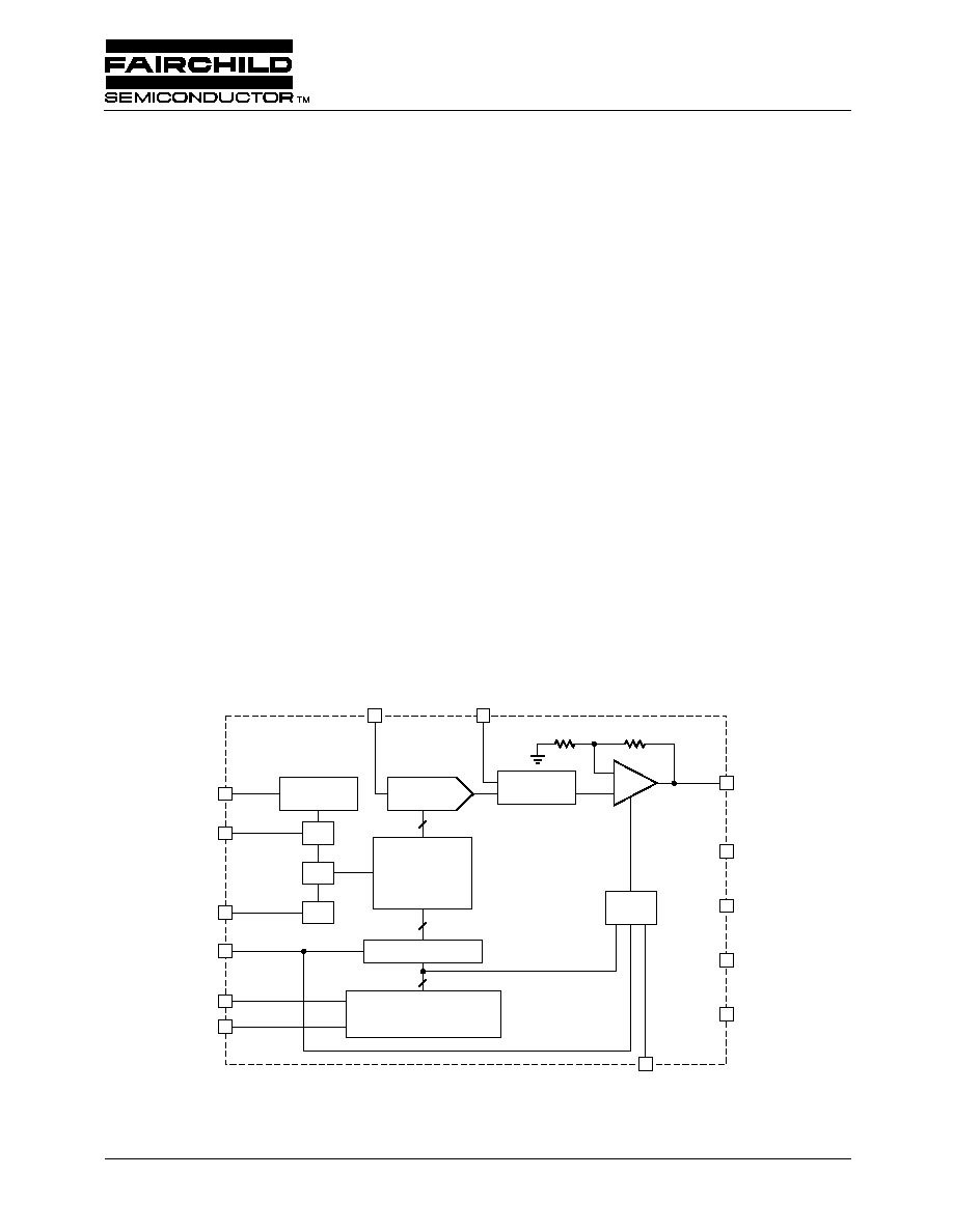
The ML2036 is a monolithic sine wave generator whose
output is programmable from DC to 50kHz. No external
components are required. The frequency of the sinewave
output is derived from either an external crystal or clock
input, providing a stable and accurate frequency reference.
The frequency is programmed by a 16-bit serial data word.
The ML2036 provides for a V
OUT
amplitude of either ±V
REF
or ±V
REF
/2. Also included with the ML2036 is an inhibit
function which allows the sinewave output to be held at zero
volts after completing the last half cycle of the sine wave in
progress. Two digital clock outputs are provided to drive
other devices with one half or one eighth of the input clock
frequency.
The ML2036 is intended for telecommunications and
modem applications that need low cost and accurate genera-
tion of precise test tones, call progress tones, and signaling
tones.
Block Diagram
(Pin configuration shown for 14-Pin PDIP Version)
CLK OUT 2
CLK OUT 1
V
OUT
LATI
SCK
SID
7
5
3
10
8-BIT
DAC
PHASE
ACCUMULATOR
& 512 POINT
SINE LOOK-UP
TABLE
8
16
16
16-BIT DATA LATCH
16-BIT SHIFT REGISTER
CRYSTAL
OSCILLATOR
÷2
CLK IN
14
AGND
11
V
CC
8
12
-
+
5k
5k
ZERO
DETECT
SMOOTHING
FILTER
÷2
÷2
4
3
DGND
V
SS
1
2
P
DN
-INH
V
REF
9
GAIN
13
ML2036
Serial Input Programmable Sine Wave Generator
with Digital Gain Control
ML2036
PRODUCT SPECIFICATION
2
REV. 1.0.2 7/26/01
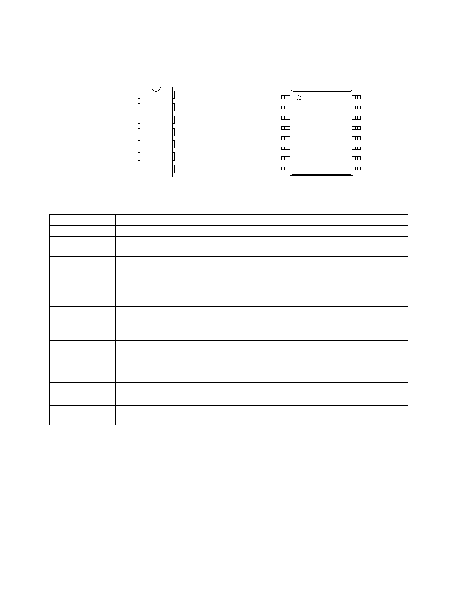
Pin Configuration
Pin Description
(Pin Number in Paranthesis is for SOIC Version)
PIN NAME
FUNCTION
1 (2)
V
SS
Negative supply (-5V).
2 (3)
P
DN
-INH
Three level input which controls the inhibit and power down modes. Current source pull-up
to V
CC
.
3 (4)
CLK
OUT 1
Digital clock output from the internal clock generator that can drive other devices at f
CLK OUT
1
= f
CLK IN
/2.
4 (5)
CLK
OUT 2
Digital clock output from the internal clock generator that can drive other devices at f
CLK OUT
2
= f
CLK IN
/8.
5 (6)
SCK
Serial clock. Digital input which clocks in serial data on its rising edges.
6 (7)
SID
Serial input data which programs the frequency of V
OUT
.
7 (8)
LATI
Digital input which latches serial data into the internal data latch on falling edges.
8 (9)
V
CC
Positive supply (5V).
9 (10)
V
REF
Reference input. The voltage on this pin determines the peak-to-peak swing of V
OUT
. V
REF
can be tied to V
CC
.
10 (11)
V
OUT
Analog output.
11 (12)
AGND
Analog ground. All analog inputs and outputs are referenced to this point.
12 (13)
DGND
Digital ground. All digital inputs and outputs are referenced to this point.
13 (15)
GAIN
Sets V
OUT
peak amplitude to V
REF
or V
REF
/2. Current source pull-down to DGND.
14 (16)
CLK IN
Clock input. The internal clock can be generated by tying a 3 to 12MHz crystal from this pin
to DGND, or by applying a digital clock signal directly to the pin.
1
2
3
4
5
6
7
14
13
12
11
10
9
8
VSS
PDN-INH
CLK OUT 1
CLK OUT 2
SCK
SID
LATI
CLK IN
GAIN
DGND
AGND
VOUT
VREF
VCC
TOP VIEW
ML2036
14-Pin PDIP (P14)
1
2
3
4
5
6
7
8
16
15
14
13
12
11
10
9
TOP VIEW
ML2036
16-Pin Wide SOIC (S16W)
NC
VSS
PDN-INH
CLK OUT 1
CLK OUT 2
SCK
SID
LATI
CLK IN
GAIN
NC
DGND
AGND
VOUT
VREF
VCC
PRODUCT SPECIFICATION
ML2036
REV. 1.0.2 7/26/01
3
Absolute Maximum Ratings
Absolute maximum ratings are those values beyond which the device could be permanently damaged. Absolute maximum
ratings are stress ratings only and functional device operation is not implied.
Operating Conditions
Parameter
Min.
Max.
Units
V
CC
6.5
V
V
SS
-6.5
V
V
OUT
V
SS
- 0.3
V
CC
+ 0.3
V
Voltage on any other pin
GND - 0.3
V
CC
+ 0.3
V
Input Current
±25
mA
Junction Temperature
150
°C
Storage Temperature Range
65
150
°C
Lead Temperature (Soldering, 10 sec)
260
°C
Thermal Resistance (
JA
)
14-Pin PDIP
16-Pin Wide SOIC
88
105
°C/W
°C/W
Parameter
Min.
Max.
Units
Temperature Range
ML2036CX
ML2036IX
0
-40
70
85
°C
°C
V
CC
Range
4.5
5.5
V
V
SS
Range
-4.5
-5.5
V
Electrical Characteristics
Unless otherwise specified, V
CC
= 4.5V to 5.5V, V
SS
= -4.5V to -5.5V, V
REF
= 2.5V to V
CC
, CLK IN = 12.352MHz,
C
L
= 100pF, R
L
= 1k
, T
A
= Operating Temperature Range (Note 1)
Symbol
Parameter
Conditions
Min.
Typ.
Max.
Units
Output
HD
Harmonic Distortion (Note 2)
(2nd and 3rd Harmonic)
20Hz to 5kHz
-45
dB
5kHz to 50kHz
-40
dB
SND
Signal to Noise + Distortion
(Note 2)
200Hz to 3.4kHz,
f
OUT
BW = 200Hz to 4kHz
-45
dB
20Hz to 50kHz,
f
OUT
BW = 20 Hz to 150kHz
-40
dB
V
GN
Gain Error (Note 2)
20Hz < f
OUT
< 5kHz
±0.15
dB
5kHz < f
OUT
< 50kHz
±0.3
dB
ICN
Idle Channel Noise
Power Down Mode, Cmsg
Weighted
-20
0
dBrnc
Power Down Mode, 1kHz
50
nV/ Hz
Inhibit Mode, 1kHz
500
nV/ Hz
PSRR
Power Supply Rejection Ratio
200mV
P-P
, 0 - 10kHz
Sine, Measured on
V
OUT
V
CC
-40
dB
V
SS
-40
dB
V
OS
V
OUT
Offset Voltage (Note 3)
±(2.5+
V
P-P
)/100
V
V
P-P
Peak-to-Peak Output Voltage
(Note 2)
GAIN = V
CC
±V
REF
V
GAIN = DGND
±V
REF
/2
V
V
OUT
Swing
GAIN = V
CC
V
SS
+1.5
V
CC
-1.5
V
R
REF
Reference Input Resistance
1
6
M
ML2036
PRODUCT SPECIFICATION
4
REV. 1.0.2 7/26/01
Notes:
1. Limits are guaranteed by 100% testing, sampling, or correlation with worst case test conditions.
2. Maximum peak-to-peak voltage for the output sine wave is: V
OUT(P-P)
(125kV x Hz)/f
OUT
. For example, at 50kHz,
the maximum output voltage swing is 2.5V
P-P
.
3. Offset voltage is a function of the peak-to-peak output voltage. For example, if V
OUT(P-P)
= 2.5V, V
OS
= ±50mV max.
Oscillator
V
IL
CLK
CLK IN Input Low Voltage
1.5
V
V
IH
CLK
CLK IN Input High Voltage
3.5
V
I
IL
CLK
CLK IN Input Low Current
-250
µA
I
IH
CLK
CLK IN Input High Current
250
µA
C
IN
CLK
CLK IN Input Capacitance
12
pF
t
CKI
CLK IN On/Off Period
t
R
= t
F
= 10ns, 2.5V Midpoint
30
ns
CLK OUT 1/CLK IN Frequency
Ratio
See Figure 2
0.49
0.51
CLK OUT 2/CLK IN Frequency
Ratio
See Figure 2
0.122
0.128
t
1R
, t
2R
CLK OUT 1, CLK OUT 2 Rise
Time
C
L
= 40pF, 10% to 90%
20
ns
C
L
= 100pF, 0.8V to 2.0V
Transition
20
ns
t
1F
, t
2F
CLK OUT 1, CLK OUT 2 Fall
Time
C
L
= 40pF, 90% to 10%
20
ns
C
L
= 100pF, 2.0V to 0.8V
Transition
20
ns
Logic
V
IL
Input Low Voltage (LATI, SCK,
SID, GAIN)
0.8
V
V
IH
Input High Voltage (LATI, SCK,
SID, GAIN)
2.0
V
V
I1
Input Low Voltage - P
DN
-INH
-0.5
0.8
V
V
I2
Inhibit Stage Voltage - P
DN
-INH
V
SS
+ 0.5
V
V
I3
Input High Voltage - P
DN
-INH
2.0
V
I
IL
-P
DN
P
DN
-INH Input Low Current
P
DN
-INH = 0V
-70
-20
-5
µA
I
IH
-GAIN
GAIN Input High Current
GAIN = V
CC
5
20
70
µA
I
IL
Input Low Current (LATI, SCK,
SID, GAIN)
V
IN
= 0V
-1
µA
I
IH
Input High Current (LATI, SCK,
SID, GAIN)
V
IN
= V
CC
1
µA
C
IN
Input Capacitance
5
pF
V
OL
Output Low Voltage
I
OL
= -2mA
0.4
V
V
OH
Output High Voltage
I
OH
= 2mA
4.0
V
t
SCK
Serial Clock On/Off Period
100
ns
t
DS
SID Data Setup Time
50
ns
t
DH
SID Data Hold Time
50
ns
t
LPW
LATI Pulse Width
50
ns
t
LH
LATI Hold Time
50
ns
t
LS
LATI Setup Time
50
ns
Supply
I
CC
V
CC
Current
No Load, V
CC
= V
REF
= 5.5V
5.5
mA
No Load, Power Down Mode
2
mA
I
SS
V
SS
Current
No Load, V
CC
= V
REF
=
5.5V, V
SS
= -5.5V
-3.5
mA
No Load, Power Down Mode
-100
µA
Electrical Characteristics
(continued)
Unless otherwise specified, V
CC
= 4.5V to 5.5V, V
SS
= -4.5V to -5.5V, V
REF
= 2.5V to V
CC
, CLK IN = 12.352MHz,
C
L
= 100pF, R
L
= 1k
, T
A
= Operating Temperature Range (Note 1)
Symbol
Parameter
Conditions
Min.
Typ.
Max.
Units
PRODUCT SPECIFICATION
ML2036
REV. 1.0.2 7/26/01
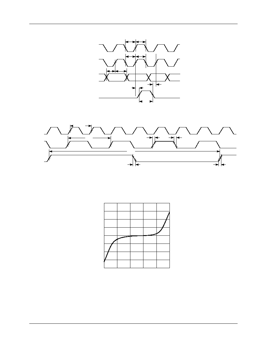
5
Figure 1. Serial Interface Timing.
Figure 2. Digital Clock Output Timing
Figure 3. CLK IN Input Current vs. Input Voltage.
CLK IN
SCK
SID
LATI
t
LPW
t
LS
t
LH
t
DS
t
DH
t
SCK
t
SCK
t
CKI
t
CKI
f
CLK1
f
CLKIN
f
CLK2
t
1R
t
1F
t
2F
t
2R
f
CLK
PARAMETERS REFERRED TO 1.4V MIDPOINT
CLK
IN
CLK
OUT
1
CLK
OUT
2
100
75
50
25
0
-25
-50
-75
-100
INPUT CURRENT (
µ
A)
INPUT VOLTAGE (V)
0
1
3
5
4
2