 | ÐлекÑÑоннÑй компоненÑ: ML4425IS | СкаÑаÑÑ:  PDF PDF  ZIP ZIP |
Äîêóìåíòàöèÿ è îïèñàíèÿ www.docs.chipfind.ru
www.fairchildsemi.com
REV. 1.0.2 7/2/01
Features
· Stand-alone operation
· Motor starts and stops with power to IC
· On-board start sequence: Align
Ramp
Set Speed
· Patented Back-EMF commutation technique provides
jitterless torque for minimum "spin-up" time
· Onboard speed control loop
· PLL used for commutation provides noise immunity from
PWM spikes, compared to noise sensitive zero crossing
technique
· PWM control for maximum efficiency
· Direct FET drive for 12V motors; drives high voltage
motors with IC buffers
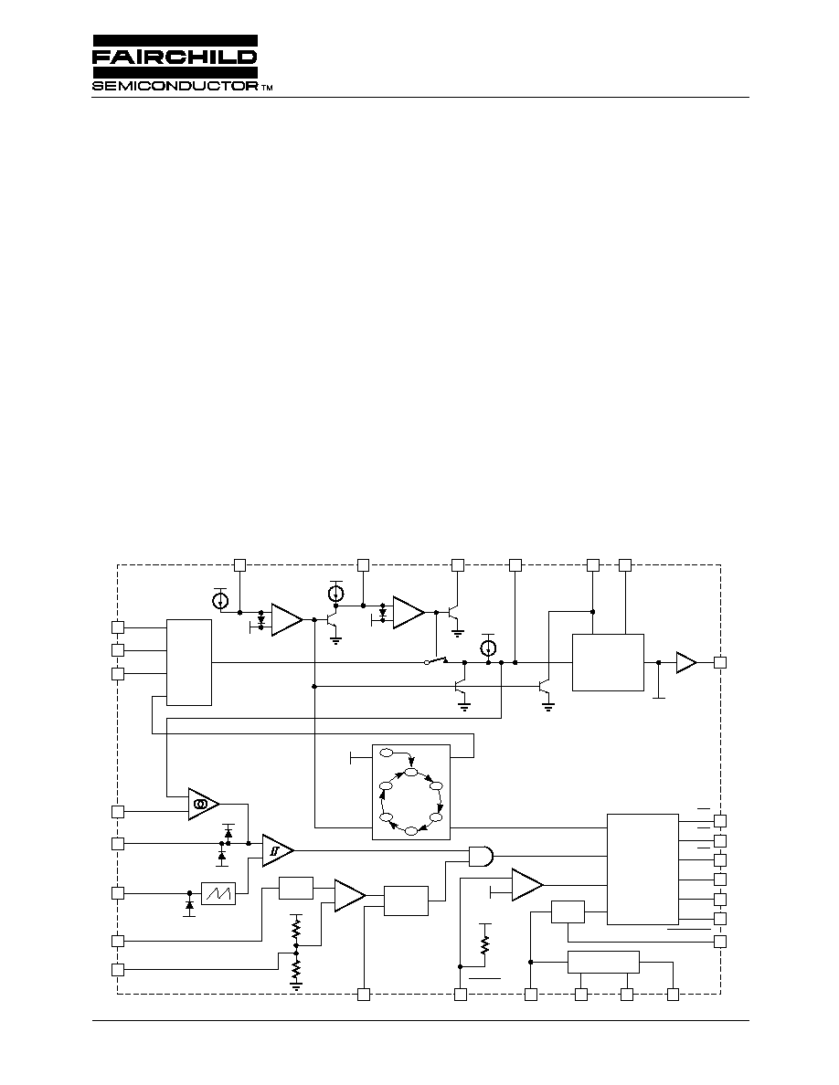
General Description
The ML4425 PWM motor controller provides all of the
functions necessary for starting and controlling the speed of
delta or wye wound Brushless DC (BLDC) motors without
Hall Effect sensors. Back EMF voltage is sensed from the
motor windings to determine the proper commutation phase
sequence using a PLL. This patented sensing technique will
commutate a wide range of 3-Phase BLDC motors and is
insensitive to PWM noise and motor snubbing circuitry.
The ML4425 limits the motor current using a constant off-
time PWM control loop. The velocity loop is controlled with
an onboard amplifier. The ML4425 has circuitry to ensure
that there is no shoot-through in directly driven external
power MOSFETs.
The timing of the start-up sequence is determined by the
selection of three timing capacitors. This allows optimization
for a wide range of motors and loads.
Block Diagram
CAT
17
FB A
22
FB B
23
FB C
24
BACK
EMF
SAMPLER
CRT
19
+
+
1.5V
750nA
+
1.5V
750nA
VDD
VDD
CRR
21
500nA
VDD
SPEED
FB
20
CVCO
15
16
RVCO
VOLTAGE
CONTROLLED
OSCILLATOR
VCO/TACH
13
2
4
3
9
10
HA
HB
HC
LA
LB
GATING
LOGIC
&
OUTPUT
DRIVERS
+
SPEED SET
8
5
SPEED COMP
3.9V
1.7V
20kHz
6
CT
+
1.4V
1
ISENSE
× 5
UVLO
12
ILIMIT
+
1.7V
VREF
26
CIOS
16k
8k
ILIMIT
1-SHOT
25
BRAKE
VDD
4k
14
VDD
28
GND
27
RREF
11
LC
REFERENCE
VCO
OUT
VCO
OUT
18
UV FAULT
7
VREF
A
B
C
D
E
F
R
COMMUTATION
STATE MACHINE
ML4425
Sensorless BLDC Motor Controller
ML4425
PRODUCT SPECIFICATION
2
REV. 1.0.2 7/2/01
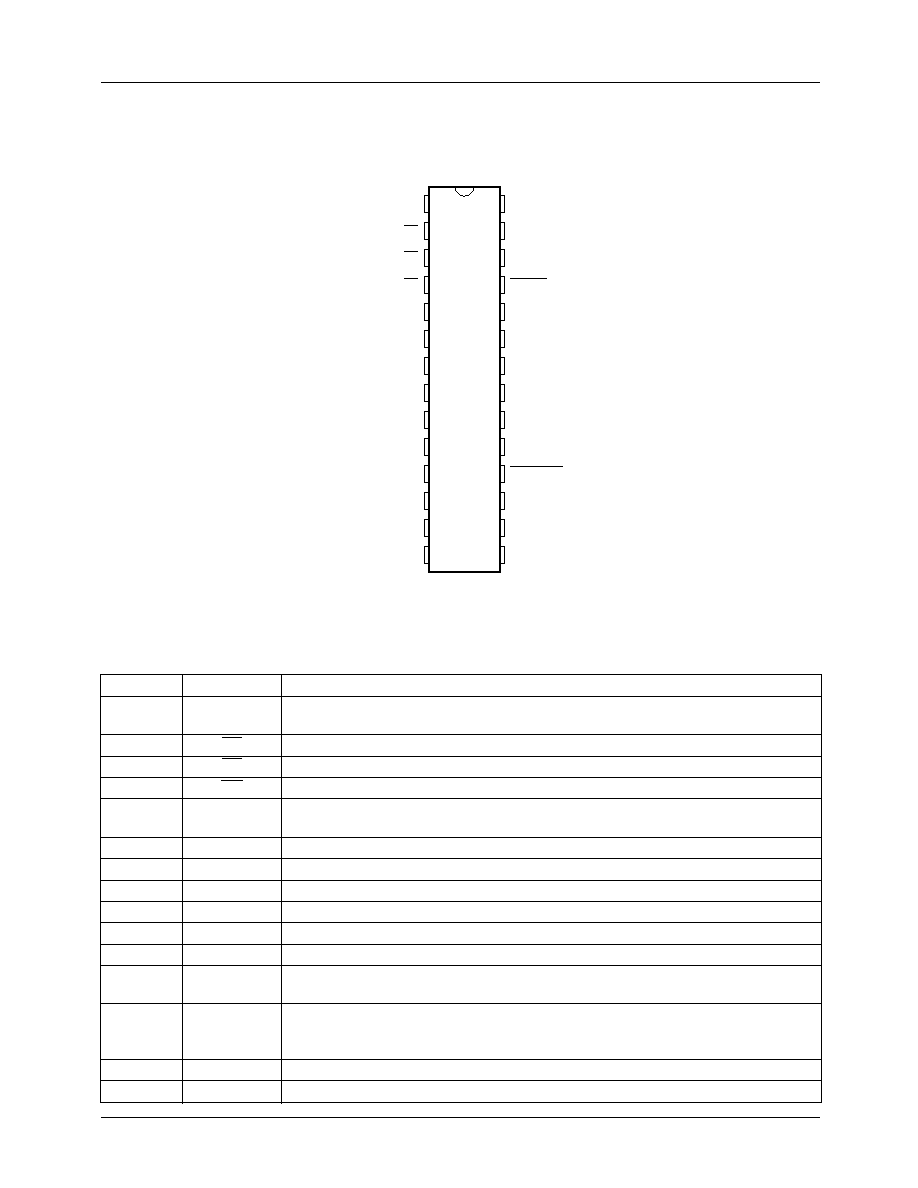
Pin Description
Pin Name
Function
1
I
SENSE
Motor current sense input. When I
SENSE
exceeds 0.2
I
LIMIT,
the output drivers LA,
LB, and LC are shut off for a fixed time determined by C
IOS
.
2
HA
Active low output driver for the phase A high-side switch.
3
HB
Active low output driver for the phase B high-side switch.
4
HC
Active low output driver for the phase C high-side switch.
5
SPEED
COMP
Speed control loop compensation is set by a series resistor and capacitor from
SPEED COMP to GND.
6
C
T
A capacitor from C
T
to GND sets the PWM oscillator frequency.
V
REF
6.9V reference voltage output.
8
SPEED SET
Speed loop input which ranges from 0 (stopped) to V
REF
(maximum speed).
9
LA
Active high output driver for the phase A low-side switch.
10
LB
Active high output driver for the phase B low-side switch.
11
LC
Active high output driver for the phase C low-side switch.
12
I
LIMIT
Voltage on this pin sets the I
SENSE
threshold voltage at 0.2
I
LIMIT
, leaving this pin
unconnected selects an internally set threshold.
13
VCO/TACH
This TTL level output corresponds to the signal used to clock the commutation state
machine. The output frequency is proportional to the motor speed when the back-
EMF sensing loop is locked onto the rotor position.
14
V
DD
12V power supply input.
15
C
VCO
A capacitor to GND sets the voltage-to-frequency ratio of the VCO.
Pin Configuration
1
2
3
4
5
6
7
8
9
10
11
12
13
14
28
27
26
25
24
23
22
21
20
19
18
17
16
15
ISENSE
HA
HB
HC
SPEED COMP
CT
VREF
SPEED SET
LA
LB
LC
ILIMIT
VCO/TACH
VDD
GND
RREF
CIOS
BRAKE
FB C
FB B
FB A
CRR
SPEED FB
CRT
UV FAULT
CAT
RVCO
CVCO
TOP VIEW
ML4425
28-Pin Narrow PDIP (P28N)
28-Pin SOIC (S28)
PRODUCT SPECIFICATION
ML4425
REV. 1.0.2 7/2/01
3
Absolute Maximum Ratings
Absolute maximum ratings are those values beyond which the device could be permanently damaged. Absolute maximum
ratings are stress ratings only and functional device operation is not implied.
Operating Conditions
16
R
VCO
An resistor to GND sets up a current proportional to the input voltage of the VCO.
17
C
AT
A capacitor to GND sets the time that the controller stays in the align mode.
18
UV FAULT
This output goes low when V
DD
drops below the UVLO threshold, and indicates that
all output drivers have been disabled.
19
C
RT
A capacitor to GND sets the time that the controller stays in the ramp mode.
20
SPEED FB
Output of the back-EMF sampling circuit and input to the VCO. An RC network
connected to SPEED FB sets the compensation for the PLL loop formed by the
back-EMF sampling circuit, the VCO, and the commutation state machine.
21
C
RR
A capacitor to between C
RR
and SPEED FB sets the ramp rate (acceleration) of the
motor when the controller is in ramp mode.
22
FB A
The motor feedback voltage from phase A is monitored through a resistor divider for
back-EMF sensing at this pin.
23
FB B
The motor feedback voltage from phase B is monitored through a resistor divider for
back-EMF sensing at this pin.
24
FB C
The motor feedback voltage from phase C is monitored through a resistor divider for
back-EMF sensing at this pin.
25
BRAKE
A logic low input activates motor braking by shutting off the high-side output drivers
and turning on the low-side output drivers.
26
C
IOS
A capacitor to GND sets the time that the low-side output drivers remain off after
I
SENSE
exceeds its threshold .
27
R
REF
An 137k
resistor to GND sets a current proportional to V
REF
that is used to set all
the internal bias currents except for the VCO.
28
GND
Signal and power ground.
Parameter
Min.
Max.
Units
V
DD
14
V
Logic Inputs (SPEED FB, BRAKE)
GND 0.3
7
V
All Other Inputs and Outputs
GND 0.3
V
DD
+ 0.3
V
Output Current (LA, LB, LC, HA, HB, HC
)
±50
mA
Junction Temperature
150
°C
Storage Temperature Range
-65
150
°C
Lead Temperature (Soldering 10 sec.)
260
°C
Thermal Resistance (
JA
)
28-Pin Narrow PDIP
28-Pin SOIC
48
75
°C/W
°C/W
Parameter
Min.
Max.
Units
Temperature Range
ML4425CX
ML4425IX
0
40
70
85
°C
°C
V
DD
10.8
13.2
V
Pin Description
(continued)
Pin Name
Function
ML4425
PRODUCT SPECIFICATION
4
REV. 1.0.2 7/2/01
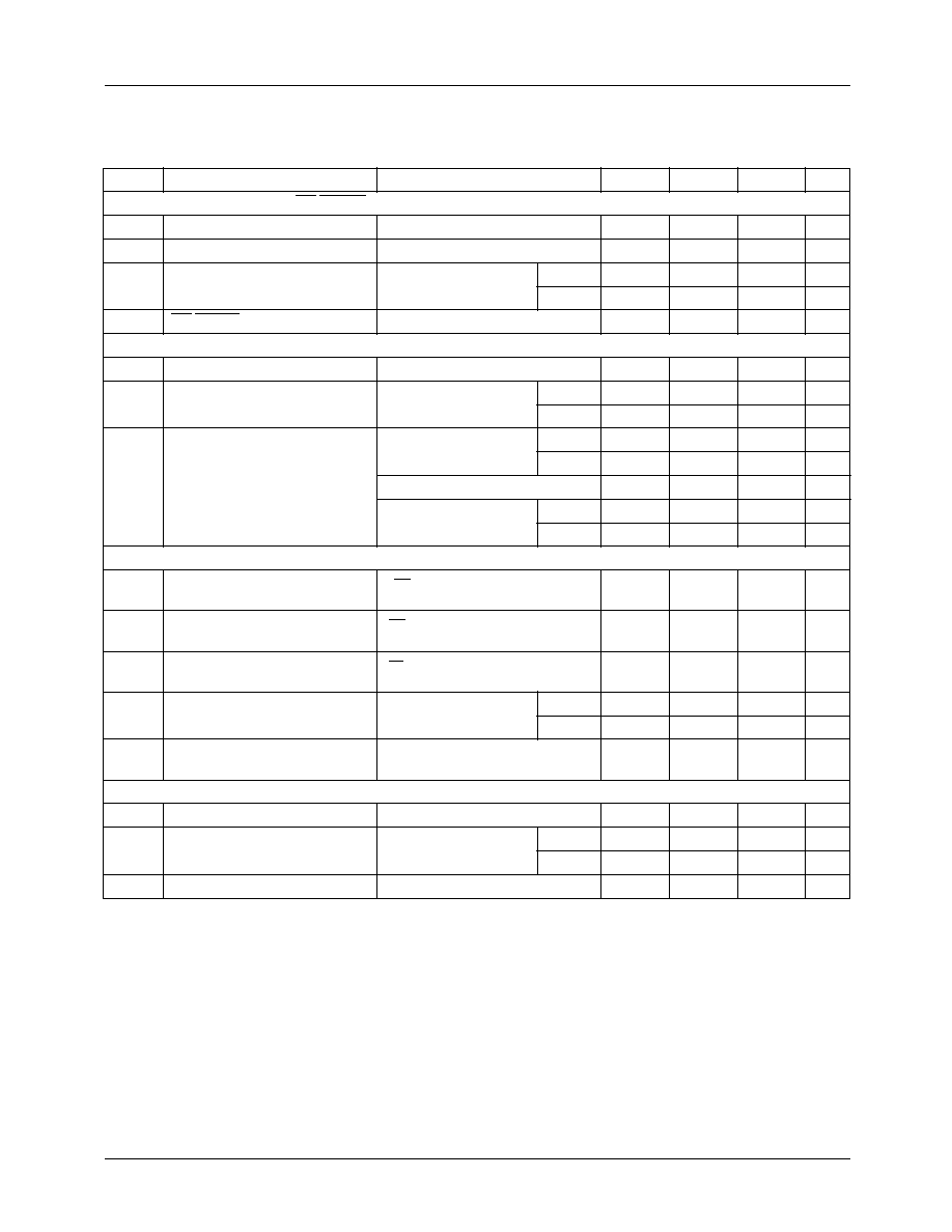
Electrical Characteristics
Unless otherwise specified, V
DD
= 12V ± 10%, R
SENSE
= 1
, C
VCO
= 10nF, C
IOS
= 100pF, R
REF
= 137k
,
T
A
= Operating Temperature Range (Notes 1, 2)
.
Symbol
Parameter
Conditions
Min.
Typ.
Max.
Units
Reference
V
REF
Total Variation
Line, Temp
6.5
6.9
7.5
V
PWM Oscillator
Total Variation
C
T
= 1nF
28
kHz
Ramp Peak
3.9
V
Ramp Valley
1.7
V
Ramp Charging Current
µA
Speed Control Loop
SPEED SET Input Voltage
Range
0
V
REF
V
SPEED FB Input Voltage Range
0
V
REF
V
SPEED COMP Output Current
±5
±20
µA
SPEED SET Error Amp
Transconductance
V
SPEED SET
= xV,
V
SPEED FB
= yV
144
µ
Start-up
C
AT
Charging Current
C Suffix
0.68
0.98
µA
I Suffix
0.5
1.1
µA
C
AT
Threshold Voltage
1.4
1.7
V
C
RT
Charging Current
C Suffix
0.68
0.98
µA
I Suffix
0.5
1.1
µA
C
RT
Threshold Voltage
1.4
1.7
V
Voltage Controlled Oscillator
Frequency Range
R
VCO
= 5V, SPEED FB = 6V
1.5
1.85
2.2
kHz
Frequency vs. SPEED FB
R
VCO
= 5V, 0.5V
SPEED FB
7V
300
Hz/V
Current Limit
I
SENSE
Gain
V(I
LIMIT
)
2.5V
4.5
5.0
5.5
V/V
One Shot OFF-Time
C
IOS
= 100pF
C Suffix
9
18
µs
I Suffix
9
20
µs
Logic Inputs (BRAKE) (Note 3)
V
IH
Input High Voltage
2
V
V
IL
Input Low Voltage
0.8
V
I
IH
Input High Current
V
IH
= 2.4V
2.4
mA
I
IL
Input Low Current
V
IL
= 0.4V
2.9
mA
PRODUCT SPECIFICATION
ML4425
REV. 1.0.2 7/2/01
5
Notes:
1. Limits are guaranteed by 100% testing, sampling, or correlation with worst case test conditions.
2. For explanation of states, see Figure 4 and Table 1.
3. The BRAKE and UV FAULT pins each have an internal 4k
resistor to the internal reference.
Logic Outputs (VCO/TACH, UV FAULT) (Note 3)
VCO/TACH Output High Voltage I
OUT
= 100µA
2.2
V
VCO/TACH Output Low Voltage
I
OUT
= 400µA
0.6
V
UV FAULT Output High Voltage
I
OUT
= 10µA
C Suffix
3.4
4.5
5.4
V
I Suffix
3.2
5.6
V
UV FAULT Output Low Voltage
I
OUT
= 400µA
0.6
V
Back-EMF Sampler
SPEED FB Align Mode Voltage
125
250
mV
SPEED FB Ramp Mode Current
C Suffix
500
720
nA
I Suffix
500
750
nA
SPEED FB Run Mode Current
State A, C
RT
= 5V,
V
PHB
= V
DD
/3
C Suffix
30
90
µA
I Suffix
27
90
µA
State A, C
RT
= 5V, V
PHB
= V
DD
/2
15
15
µA
State A, C
RT
= 5V,
V
PHB
= 2
V
DD
/3
C Suffix
90
30
µA
I Suffix
90
27
µA
Output Drivers
High Side Driver Output Low
Current
V
HX
= 2
V
0.5
1.2
mA
High Side Driver Output High
Voltage
I
HX
= 10µ
A
V
CC
1.3
V
Low Side Driver Output Low
Voltage
I
LX
= 1mA
0.2
0.7
V
Low Side Driver Output High
Voltage
V(I
SENSE
) = 0V
C Suffix V
DD
2.2
V
I Suffix
V
DD
2.9
V
Phase C Cross-conduction
Lockout Threshold
V
DD
3.0
V
Supply
I
DD
V
DD
Current
32
50
mA
UVLO Threshold
C Suffix
8.8
9.5
10.2
V
I Suffix
8.6
10.3
V
UVLO Hysteresis
150
mV
Electrical Characteristics
(continued)
Unless otherwise specified, V
DD
= 12V ± 10%, R
SENSE
= 1
, C
VCO
= 10nF, C
IOS
= 100pF, R
REF
= 137k
,
T
A
= Operating Temperature Range (Notes 1, 2).
Symbol
Parameter
Conditions
Min.
Typ.
Max.
Units